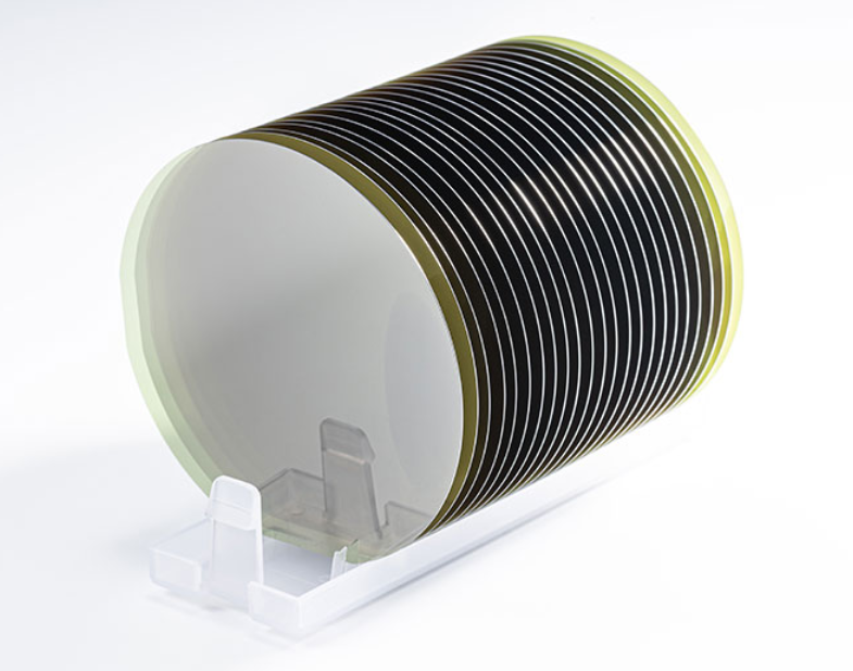
In the semiconductor manufacturing field, wafer thinning is a crucial process. It involves reducing the thickness of semiconductor wafers through methods such as mechanical grinding, chemical mechanical polishing (CMP), or chemical etching. This article explores the necessity of wafer thinning, the methods employed, and its significant role in the semiconductor industry.
Why is Wafer Thinning Necessary?
Wafer thinning is not merely a physical process; it holds substantial importance for several reasons:
1. Improved Thermal Management
As chip functionality and integration increase, thermal management becomes increasingly critical. Thinning the wafer allows for more effective heat conduction and dissipation, thereby enhancing the reliability and performance of the devices. This is especially crucial for high-performance computing and high-power electronic devices.
2. Enhanced Packaging Density
Thinning the wafer allows chips to be packaged more densely, contributing to the development of smaller and lighter electronic products. This is particularly important for mobile devices such as smartphones and tablets, which have stringent requirements for size and weight.
3. Increased Mechanical Flexibility
Thin wafers exhibit better mechanical flexibility, allowing them to withstand greater bending and pressure. This is significant for certain flexible electronics or three-dimensional packaging technologies (such as TSV, Through-Silicon Via), enabling devices to maintain performance while enhancing mechanical resilience.
4. Reduced Production Costs
By thinning the wafer, more chips can be processed from a single wafer, improving material utilization and thereby reducing the production cost per chip. This is advantageous for the large-scale production of semiconductor devices, significantly enhancing manufacturing efficiency.
5. Support for Advanced Packaging Technologies
Wafer thinning is a key step for many advanced packaging technologies, such as stacked chips and system-in-package (SiP). Thin wafers allow for the stacking of multiple chip layers, improving integration and performance. This is crucial for modern electronic products that continuously pursue higher performance and more functions.

The Wafer Thinning Process
The wafer thinning process typically includes the following steps:
1. Coarse Grinding: Using coarse abrasives to quickly remove a large amount of material, reducing the wafer thickness to near the target thickness.
2. Fine Grinding: Using finer abrasives for further grinding to achieve the precise thickness requirement.
3. Chemical Mechanical Polishing (CMP): Combining chemical and mechanical methods to remove a small amount of material, achieving a very smooth and uniform surface.
Conclusion
Wafer thinning plays an indispensable role in semiconductor manufacturing. From improving thermal management to supporting advanced packaging technologies, the advantages of wafer thinning significantly enhance chip performance and reliability. As electronic products continue to trend towards miniaturization, high performance, and multi-functionality, the importance of wafer thinning technology will become increasingly prominent. In the future, with continuous technological advancements, wafer thinning processes will further optimize, bringing more innovation and breakthroughs to the semiconductor industry.
Related product links
Silicon Carbide Wafer (SiC Wafer)
With the continuous advancement of power electronics, RF devices, and optoelectronic technologies, the demand ...
The selection of substrate materials plays a crucial role in the development of high-frequency, high-power RF ...
IntroductionSilicon carbide (SiC), gallium nitride (GaN), and sapphire (Al₂O₃) are essential materials in semi...