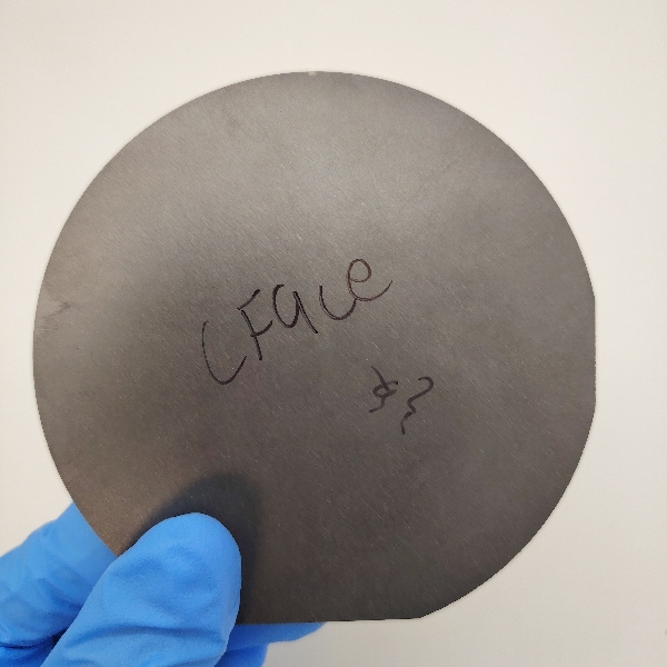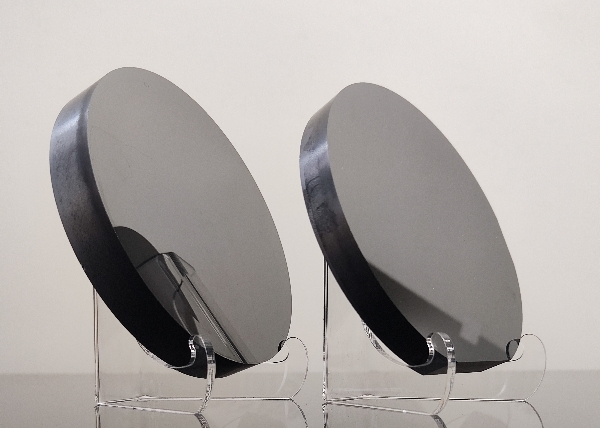
In semiconductor wafer manufacturing, material removal techniques play a critical role. The three commonly used techniques are Grinding, CMP (Chemical Mechanical Polishing), and MP (Mechanical Polishing). Although all involve material removal, their principles, application scenarios, and effects differ. This article will explore the connections and differences between these three techniques.
Grinding
Grinding is a technique that involves the rough removal of material from a wafer through mechanical means. Its main characteristics and applications include:
1. Mechanical Removal: Grinding uses grinding wheels or abrasives to remove material through mechanical abrasion.
2. Efficient Thinning: This technique is primarily used to thin thick wafers to the desired thickness, typically in the early stages of wafer manufacturing.
3. Large Material Removal: Grinding can remove a large amount of material in a short time, making it highly efficient but resulting in a rough surface finish.
4. Subsequent Processing: Due to the high surface roughness, grinding usually requires subsequent polishing steps (such as CMP or MP) to improve surface quality.

CMP (Chemical Mechanical Polishing)
CMP, or Chemical Mechanical Polishing, is a technique that combines chemical corrosion and mechanical polishing for fine surface planarization. Its main characteristics and applications include:
1. Combination of Chemical and Mechanical: CMP uses chemical agents (such as etchants) and mechanical abrasives to remove material. The chemical agents soften or dissolve the surface material, while mechanical abrasives remove these softened materials through physical friction.
2. High Precision Planarization: CMP can precisely control the thickness of the removed material, achieving high surface flatness and smoothness.
3. Critical Process Steps: This technique is widely used in critical process steps such as multilayer metal interconnects and shallow trench isolation (STI), where high precision and high flatness are required.
MP (Mechanical Polishing)
MP, or Mechanical Polishing, is a purely mechanical material removal technique that directly removes surface material through mechanical friction. Its main characteristics and applications include:
1. Pure Mechanical Process: MP relies solely on mechanical friction to remove surface material without using chemical agents.
2. Rough Polishing: This technique is typically used for non-critical steps or preliminary polishing, where precision control is lower.
3. Lower Cost: MP is relatively low-cost since it does not require expensive chemical agents.
4. Application Limitations: Due to its lower control precision and planarization effect compared to CMP, MP is mainly used for coarse polishing or bulk material removal, often serving as a pre-treatment step before CMP.

Connections and Differences
1. Material Removal Methods:
Grinding: Uses purely mechanical methods, high efficiency, large removal volume, but rough surface.
CMP: Combines chemical and mechanical methods, high precision removal, and good surface flatness.
MP: Relies on purely mechanical methods, lower precision removal, and lower cost.
2. Application Scenarios:
Grinding: Used for wafer thinning and initial shaping, typically requiring subsequent polishing.
CMP: Used for critical process steps requiring high precision and high flatness.
MP: Used for preliminary or non-critical polishing steps, often as a pre-treatment for CMP.
3. Surface Quality:
Grinding: Results in a rough surface, requiring further polishing.
CMP: Produces a smooth and highly flat surface.
MP: Produces a relatively rough surface, with lower flatness and smoothness compared to CMP.
Conclusion
Grinding, CMP, and MP each have their unique roles and advantages in wafer manufacturing. Grinding is primarily used for initial rough material removal and efficient thinning. CMP is employed for critical steps, achieving high precision and high flatness surface treatment. MP is used for non-critical or preliminary polishing steps, often serving as a pre-treatment for CMP. Understanding the characteristics and application scenarios of these techniques helps optimize semiconductor manufacturing processes, enhancing production efficiency and product quality.
Related product links
Silicon Carbide Wafer (SiC Wafer)
As semiconductor technology advances, Gallium Nitride (GaN) has become a core material in optoelectronics, rad...
With the rapid advancement of third-generation semiconductor technologies, Silicon Carbide (SiC) has emerged a...
As third-generation semiconductor materials such as silicon carbide (SiC) and gallium nitride (GaN) continue t...
