Introduction
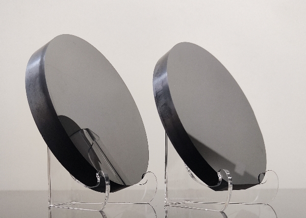
Silicon carbide (SiC), gallium nitride (GaN), and sapphire (Al₂O₃) are essential materials in semiconductor, optoelectronic, and high-power electronic devices due to their exceptional physical and chemical properties. However, their high hardness and chemical stability make processing challenging. Traditional mechanical polishing (MP) and chemical mechanical polishing (CMP) have limitations in surface quality and damage layer control. Therefore, exploring advanced polishing technologies to enhance surface quality and minimize damage layers is crucial for improving device performance.
1. Ion Beam Polishing (IBP)
Principle
Ion Beam Polishing (IBP) utilizes high-energy ion beams to bombard the wafer surface, removing microscopic surface irregularities for ultra-precise finishing. By controlling ion beam energy and angle, it effectively reduces damage layers while improving surface smoothness.
Advantages
Non-contact processing, avoiding microcracks and stress from traditional grinding.
Suitable for ultra-hard materials, such as 4H-SiC, 6H-SiC, and GaN.
Achieves atomic-level smooth surfaces (Ra < 0.1 nm).
Applications
Final polishing before SiC and GaN epitaxy, reducing dislocation density and improving epitaxial layer quality.
Ultra-precision polishing for high-end optical components.
2. Gas Cluster Ion Beam Polishing (GCIB)
Principle
GCIB uses high-density gas clusters (e.g., argon or nitrogen) to bombard the surface, enabling damage-free material removal. Compared to single-ion beams, gas cluster ion beams distribute energy more uniformly, allowing finer surface finishing.
Advantages
Completely damage-free, ideal for high-precision semiconductor and optical components.
Achieves atomic-level smoothness (Ra < 0.1 nm).
Suitable for final polishing of sapphire, SiC, and GaN.
Applications
Ultra-precision polishing before SiC and GaN epitaxy.
Surface treatment of high-end optical materials for EUV lithography.
3. Thermochemical Polishing (TCP)
Principle
Under high temperatures (typically > 1000°C), specific atmospheric conditions (such as oxygen, chlorine, or hydrogen) selectively etch the material surface while airflow or plasma smooths the surface.
Advantages
Effectively removes deep damage layers that conventional CMP struggles with.
Suitable for ultra-hard materials (SiC), particularly for power electronic substrates.
Eliminates scratches and microcracks by avoiding mechanical pressure.
Applications
Final processing of high-power SiC device substrates to enhance thermal conductivity and surface quality.
Ultra-fine polishing of high-end GaN laser substrates.
4. Ultrasonic Assisted Polishing (UAP)
Principle
During traditional CMP, ultrasonic vibrations are applied to distribute abrasive particles evenly in the polishing slurry and accelerate chemical reactions.
Advantages
Increases material removal rate (MRR), reducing polishing time and improving efficiency.
Suitable for large-diameter SiC/GaN wafer polishing.
Achieves surface roughness below 0.2 nm.
Applications
High-yield polishing of 6-8 inch SiC/GaN wafers.
Enhancing interface quality of GaN-on-SiC epitaxial wafers.
5. Magnetorheological Finishing (MRF)
Principle
MRF controls abrasive particles in a magnetic fluid using a magnetic field, enabling highly precise material removal, ideal for precision machining.
Advantages
Precisely controls material removal rate, achieving sub-nanometer flatness.
Suitable for curved or complex geometries (e.g., specialized optical lenses).
Ideal for ultra-precise optical and semiconductor components.
Applications
Ultimate polishing of high-end sapphire windows and GaN optoelectronic devices.
Sapphire substrate processing for high-power laser applications.
6. Plasma-Assisted Polishing (PAP)
Principle
Low-temperature plasma activates the wafer surface, making chemical polishing reactions more uniform and gentle, resulting in high-quality surface treatment.
Advantages
Suitable for hard materials like GaN and SiC without mechanical damage.
Can be combined with CMP for final surface correction, further enhancing smoothness.
Applicable to ultra-precision microelectronics and optical applications.
Applications
Pre-epitaxial treatment of high-end SiC/GaN devices.
Surface refinement of high-precision optical components.
Conclusion: Which Polishing Technology is Most Suitable?
| Polishing Technology | Suitable Materials | Surface Roughness (Ra) | Key Advantages |
CMP (Chemical Mechanical Polishing) | Si, SiC, GaN, Sapphire | < 0.5 nm | Mature process, suitable for mass production |
| Ion Beam Polishing (IBP) | SiC, GaN | < 0.1 nm | No mechanical damage, ideal for high-precision needs |
GCIB (Gas Cluster Ion Beam Polishing) | SiC, GaN, Sapphire | < 0.1 nm | Atomic-level smoothness, damage-free |
Thermochemical Polishing (TCP) | SiC | < 0.2 nm | High-temperature treatment, removes deep damage layers |
Ultrasonic Assisted Polishing (UAP) | SiC, GaN | < 0.2 nm | Increases removal rate, reduces processing time |
Magnetorheological Finishing (MRF) | Sapphire, Optical Lenses | < 0.2 nm | Precision control, ideal for complex surfaces |
| Plasma-Assisted Polishing (PAP) | GaN, SiC | < 0.1 nm | No mechanical damage, enhances epitaxial quality |
For large-scale production, CMP remains the mainstream choice. However, for high-end SiC/GaN epitaxial substrates, IBP, GCIB, and PAP technologies hold significant potential to improve surface quality and minimize damage layers, ultimately enhancing semiconductor device performance.
With the continuous advancement of power electronics, RF devices, and optoelectronic technologies, the demand ...
The selection of substrate materials plays a crucial role in the development of high-frequency, high-power RF ...
IntroductionSilicon carbide (SiC), gallium nitride (GaN), and sapphire (Al₂O₃) are essential materials in semi...