The fabrication of 8-inch sapphire substrates is a complex and precise process that involves several key steps. Initially, high-purity aluminum oxide (Al₂O₃) powder is used as the raw material to ensure the purity and quality of the material. Next, sapphire single crystals are grown from the molten aluminum oxide using crystal growth techniques such as the Czochralski (CZ) method, the Kyropoulos (KY) method, or the Heat Exchanger Method (HEM). This process requires stringent control of temperature and cooling rates to achieve high-quality single crystals.
Following this, a multi-wire saw is used to cut the large sapphire single crystal into uniformly thick circular wafers. Diamond wire and appropriate cutting fluids are employed to minimize damage during the cutting process. The cut wafers then undergo coarse grinding and fine grinding to remove surface damage and achieve the desired thickness and flatness. Coarse grinding typically uses large-grit diamond wheels, while fine grinding employs smaller-grit diamond wheels. Subsequently, a Chemical Mechanical Planarization (CMP) process is used to polish the wafer surface to a smooth, scratch-free mirror finish. Polishing fluids and pads are used, with careful control of polishing pressure and speed, to achieve high-quality surfaces. After polishing, the wafers are subjected to ultrasonic cleaning to remove residual polishing fluids and particles. Optical microscopy, Atomic Force Microscopy (AFM), and X-ray Diffraction (XRD) are then used to assess surface quality and structural integrity. Depending on the requirements, the wafer's back surface may undergo roughening treatment to enhance adhesion to subsequent epitaxial layers or be subjected to specific back-side coatings. Finally, the finished sapphire substrates undergo rigorous quality inspection to ensure uniform thickness, surface smoothness, and crystal integrity. Parameters such as surface roughness, warping, and particle count are meticulously measured to ensure product quality. The qualified sapphire substrates are then cleanly packaged to prevent contamination and damage during transport and storage, and shipped according to customer specifications. Through these steps, high-quality 8-inch sapphire substrates can be produced for applications in LEDs, RFICs, and other fields. Please refer to the following images for a detailed process.

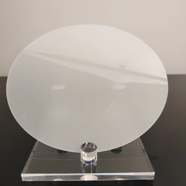
The key specifications of 8-inch sapphire substrates include the following aspects:
Dimensions and Shape: Diameter: 200 ± 0.2 mm, thickness: 1600± 25 um (adjustable). Edge shape: circular, with/without beveling. Flatness: within 5 µm.
Crystal Orientation: Common orientations are C-plane (0001), A-plane (11-20), and R-plane (1-102), with accuracy ±0.1° or better.
Surface Quality: Surface roughness (Ra) < 0.3 nm. Mirror-like polished surfaces. Warping < 15 µm, bowing < 10 µm, total thickness variation (TTV) < 10 µm.
Mechanical Strength: Sufficient to avoid breakage or damage during processing.
Transmittance: High transmittance across UV to near-IR spectrum, varying by application.
Impurities and Defects: High purity, impurities at ppm level. Minimized crystal defects for integrity.
Parallelism and Perpendicularity: Parallelism within 5 µm, edge-to-surface perpendicularity within specified limits.
Back Surface Treatment: Roughened or coated for adhesion to epitaxial layers or specific applications.
Marking and Identification: Etched or laser-etched batch numbers, orientation markers for traceability.
Refer to the table for detailed specifications.

These specifications ensure that sapphire substrates exhibit excellent performance and reliability in applications such as LEDs, RFICs, and optoelectronic devices. Different applications may have specific requirements for these specifications, and hence, precise specifications may be adjusted based on customer needs. By adhering to strict fabrication processes and controlling key specifications, high-quality 8-inch sapphire substrates can be produced to meet the needs of various advanced applications.
The next article will specifically cover the applications of 8-inch sapphire substrates, discussing their practical uses in different fields and related technical challenges.
Related product links
As semiconductor technology advances, Gallium Nitride (GaN) has become a core material in optoelectronics, rad...
With the rapid advancement of third-generation semiconductor technologies, Silicon Carbide (SiC) has emerged a...
As third-generation semiconductor materials such as silicon carbide (SiC) and gallium nitride (GaN) continue t...