With the continuous advancement of modern semiconductor technology, integrated circuits (ICs) are rapidly evolving toward higher density, miniaturization, and lower power consumption. Against this backdrop, wafer thinning technology has become increasingly crucial. Wafer thinning refers to the process of reducing the thickness of a fully processed semiconductor wafer using grinding, polishing, and other techniques. Although this process might seem straightforward, it significantly impacts the performance, packaging, and application of semiconductor devices. This article will explore the reasons for wafer thinning, the methods involved, and its importance and applications in the semiconductor industry.
What is Wafer Thinning?
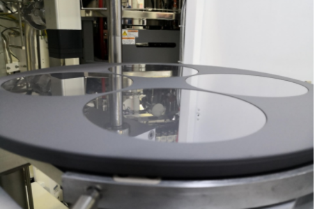
Wafer thinning is a critical process step in semiconductor manufacturing, typically performed after the wafer has completed chip fabrication and testing. It involves reducing the thickness of the wafer from the standard 500-700 micrometers to as thin as 100 micrometers or even less, using mechanical grinding and chemical mechanical polishing (CMP). Wafer thinning requires precise control to ensure uniformity and surface quality, which are essential to maintaining the integrity of the micro-circuits on the wafer.
Why Thinning Wafers is Necessary?
The need for wafer thinning arises primarily from the following considerations:
1. Enhancing Thermal Performance
The increasing integration density of modern semiconductor devices results in higher power density within the chips, leading to greater heat generation. Excessive temperatures can degrade chip performance and shorten its lifespan. By thinning the wafer, the path for heat dissipation from inside the chip to the external heat sink is shortened, thereby improving thermal efficiency. This effective heat dissipation helps maintain the chip within an optimal operating temperature range, enhancing device stability and reliability.
2. Meeting Packaging Requirements
As advanced packaging technologies evolve, such as flip-chip (FC), wafer-level packaging (WLP), and three-dimensional integrated circuits (3D ICs), wafer thinning becomes increasingly important. Thinned wafers can better accommodate these packaging technologies' requirements. For instance, in 3D integrated circuits, multiple chips are stacked together, and thinning the wafer helps reduce the thickness of each stack layer, thus minimizing the overall height of the package. This is crucial for meeting the design needs of modern electronic products, which prioritize slim and lightweight features, such as smartphones, tablets, and wearable devices.
3. Improving Mechanical Flexibility
With the rise of flexible electronics, there is a growing demand for mechanical flexibility in electronic components used in flexible displays and wearable devices. Thinned wafers offer a degree of flexibility, allowing them to withstand a certain amount of bending without damage. This characteristic makes thin wafers ideal for use in flexible circuits, flexible displays, and other applications. Through wafer thinning technology, semiconductor devices can better align with the development trend of flexible electronics.
4. Reducing Manufacturing Costs
Wafer thinning can also help reduce costs in certain cases. Firstly, thinning wafers means that more chips can be produced from the same silicon wafer, increasing material utilization. This is particularly significant when using high-cost materials such as silicon carbide and gallium arsenide, where thinning can notably reduce material consumption. Secondly, thinner wafers may require fewer consumables in some subsequent processing steps, further lowering production costs. Additionally, devices with thinned wafers are lighter, which could offer cost advantages in transportation and assembly.
5. Reducing Weight
In weight-sensitive applications, such as aerospace, satellites, and drones, reducing weight is an important design consideration. By thinning wafers, the total weight of chips and modules can be effectively reduced, meeting the requirements of these specialized applications. For some portable and mobile devices, weight reduction not only helps improve user experience but also can extend battery life.
Technical Challenges in Wafer Thinning
While wafer thinning technology offers numerous advantages, it also presents technical challenges. Thinning the wafer reduces its mechanical strength, increasing the risk of breakage. Therefore, special handling and support technologies are needed during the thinning process to prevent wafer damage. Furthermore, thinned wafers must be handled with extra care during subsequent processing and packaging to prevent breakage and warping due to their reduced thickness.
Conclusion
Wafer thinning is an indispensable step in modern semiconductor manufacturing and packaging. By enhancing thermal performance, meeting advanced packaging requirements, improving flexibility, reducing costs, and lowering weight, wafer thinning plays a vital role in advancing semiconductor technology and meeting various application needs. As technology advances and market demands continue to change, wafer thinning technology will continue to evolve, occupying an increasingly important position in future semiconductor manufacturing. For semiconductor manufacturers, mastering and optimizing this technology will be key to enhancing product competitiveness and market share.
Related product links
Silicon Carbide Wafer (SiC Wafer)
With the continuous advancement of power electronics, RF devices, and optoelectronic technologies, the demand ...
The selection of substrate materials plays a crucial role in the development of high-frequency, high-power RF ...
IntroductionSilicon carbide (SiC), gallium nitride (GaN), and sapphire (Al₂O₃) are essential materials in semi...