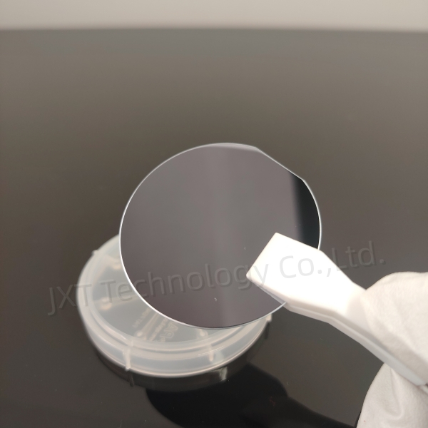
Gallium Arsenide (GaAs) wafers, as a crucial compound semiconductor material, are widely used in the production of high-performance electronic and optoelectronic devices due to their exceptional electronic and optical properties. To meet the diverse demands of various applications, GaAs wafers can be categorized based on doping methods, crystal structure, size specifications, and specific usage. This article systematically introduces the main classification methods of GaAs wafers and their corresponding application fields.
1. Classification by Doping Type
GaAs wafers can be classified into different types based on the doping elements introduced into the material:
Intrinsic GaAs Wafers (i-GaAs)
Intrinsic GaAs wafers refer to pure GaAs material without any dopants, typically featuring high resistivity. These wafers are well-suited for optoelectronic applications requiring excellent electrical performance, such as lasers and photodetectors. Due to their superior optoelectronic conversion properties, they are highly valued in optoelectronic devices.
n-type GaAs Wafers
n-type GaAs wafers are doped with elements such as silicon (Si), selenium (Se), or tin (Sn), where electrons serve as the primary charge carriers. These wafers exhibit excellent conductivity, making them ideal for high-frequency radio frequency (RF) and microwave devices, such as RF switches and power amplifiers. They are widely used in wireless communication, radar systems, and 5G base stations.
p-type GaAs Wafers
By doping GaAs wafers with elements such as zinc (Zn), magnesium (Mg), or carbon (C), holes become the primary charge carriers. p-type GaAs wafers are commonly paired with n-type wafers to form p-n junctions, which are widely used in optoelectronic devices and integrated circuits to achieve efficient electronic and photonic conversions.

2. Classification by Wafer Structure
GaAs wafers can also be categorized by their structural composition:
Single-Layer GaAs Wafers
Single-layer GaAs wafers are composed of pure GaAs material and are primarily used in the production of high-frequency and high-speed electronic devices. Due to the high electron mobility of GaAs, these wafers offer exceptional performance in high-frequency signal processing applications.
Multilayer Heterostructure GaAs Wafers
Multilayer heterostructure wafers are grown using epitaxial techniques such as Molecular Beam Epitaxy (MBE) or Metal Organic Chemical Vapor Deposition (MOCVD), where multiple layers of materials, such as GaAs/AlGaAs, are deposited on a GaAs substrate. These wafers are widely used in optoelectronic fields, including lasers, photodetectors, and high-efficiency solar cells. The heterostructure design enhances the optical and electrical performance of these devices.
3. Classification by Wafer Diameter
GaAs wafers are available in various size specifications depending on the manufacturing process:
2 inches (50.8 mm)
3 inches (76.2 mm)
4 inches (100 mm)
6 inches (150 mm)
8 inches (200 mm)
As the wafer diameter increases, the number of devices that can be fabricated per wafer also increases, which is advantageous for mass production. However, larger wafers are more difficult and costly to manufacture, requiring a balance between application demands and production costs.
4. Classification by Application
GaAs wafers can also be categorized based on their specific application fields:
Optoelectronic Wafers
GaAs wafers are extensively used in optoelectronic devices such as Light-Emitting Diodes (LEDs), Laser Diodes (LDs), and photodetectors. These devices play crucial roles in optical communication, display technologies, and optical sensors. GaAs’s high optoelectronic conversion efficiency makes it an ideal material for these applications.
Microwave and RF Wafers
In wireless communication, radar, and microwave systems, high-frequency devices such as microwave power amplifiers and Low Noise Amplifiers (LNAs) heavily rely on GaAs wafers. The high electron mobility and low noise characteristics of GaAs enable these devices to maintain stable performance in high-frequency environments.
Solar Cell Wafers
GaAs wafers are widely used in high-performance solar cells due to their high photovoltaic conversion efficiency, especially in space solar applications. The stability and high efficiency of GaAs make it the preferred material for solar cells in aerospace and satellite applications.
Conclusion
GaAs wafers, with their unique physical and electrical properties, exhibit superior performance in both electronic and optoelectronic devices. Through proper doping, structural design, and size selection, different types of GaAs wafers can meet the demands of various fields, such as high-speed electronics, microwave, and optoelectronics, driving continuous advancements in modern information and energy technologies.
You can check specific product prices for a 2-inch GaAs wafer (N-type) via this eBay link.
As semiconductor technology advances, Gallium Nitride (GaN) has become a core material in optoelectronics, rad...
With the rapid advancement of third-generation semiconductor technologies, Silicon Carbide (SiC) has emerged a...
As third-generation semiconductor materials such as silicon carbide (SiC) and gallium nitride (GaN) continue t...
