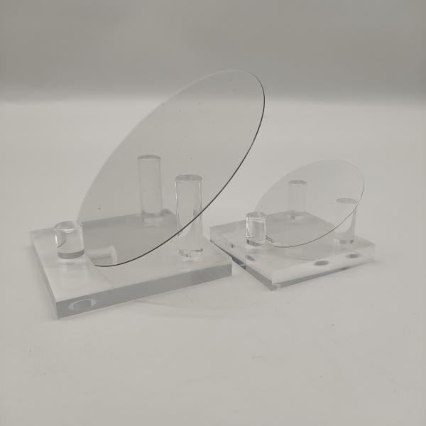
Gallium Nitride (GaN), as a core material of the third-generation wide bandgap semiconductors, is rapidly emerging as the ideal choice for optoelectronic, power electronic, and microelectronic applications due to its superior properties. GaN exhibits high breakdown field strength, high electron saturation velocity, strong radiation resistance, and excellent chemical stability, supporting a wide range of high-power and high-efficiency applications. However, despite its outstanding performance, GaN's development in practical applications has been constrained by significant technical challenges.

Advantages and Challenges of Gallium Nitride
One of the most notable advantages of GaN lies in its ability to serve as a substrate for the growth of high-quality GaN epitaxial layers. This can dramatically reduce the defect density in the epitaxial layer compared to sapphire substrates, effectively lowering the junction temperature of LEDs and increasing the brightness per unit area by over tenfold. Nevertheless, the growth of GaN single crystals is a highly challenging process. GaN cannot be melted under normal pressure and decomposes into Ga and nitrogen gas at high temperatures. This characteristic prevents the use of traditional melt methods for growing GaN single crystals, thereby limiting the size and yield of GaN crystals and driving up costs. Currently, a 2-inch GaN wafer is priced as high as $5,000 on the international market, and even at that price, supply remains tight.
Methods for Growing GaN Single Crystals
To overcome the challenges in growing GaN single crystals, both academia and industry have developed several methods, including Hydride Vapor Phase Epitaxy (HVPE), ammonothermal, and flux-based techniques. Each method has its advantages and disadvantages and has gradually been adopted in practical production.
1. Hydride Vapor Phase Epitaxy (HVPE)
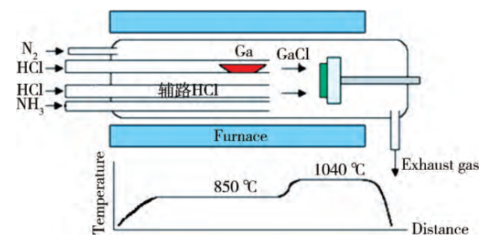
HVPE is currently the most mainstream method for growing GaN single crystal substrates. The advantages of HVPE technology include atmospheric pressure growth, fast growth rates, and the ability to achieve large-size crystal production. The HVPE system primarily consists of two reaction zones: a low-temperature zone and a high-temperature zone. In the low-temperature zone, metallic gallium reacts with hydrogen chloride to form gaseous gallium chloride (GaCl), which is then transported to the high-temperature zone by a carrier gas. In this zone, GaCl reacts with ammonia (NH3) on the substrate to deposit GaN single crystals. Due to its maturity and efficiency, HVPE has been widely adopted for commercial production.

2. Ammonothermal Method
The ammonothermal method grows GaN crystals by dissolving GaN feedstock in a supercritical ammonia solution under high temperature and pressure, and then recrystallizing it on a GaN seed crystal. This process, akin to hydrothermal growth of quartz, is carried out in an autoclave, which must be made from special materials resistant to high temperatures, high pressures, and corrosive environments. The ammonothermal method's key advantage is that it allows GaN growth at relatively low temperatures, though the high costs associated with autoclave construction and operation limit its widespread use.
3. Flux-Based Method
The flux-based method, also known as the sodium (Na) flux method, enhances nitrogen solubility in gallium by adding sodium to the gallium melt, allowing GaN growth at lower temperatures and pressures. In this process, sodium in the Ga-Na melt facilitates the ionization of nitrogen gas at the gas-liquid interface, forming nitrogen ions (N³⁻). Although nitrogen's solubility in metallic Ga and Na is low, the ionized N³⁻ increases nitrogen solubility in the melt by nearly a thousandfold. Under temperature or concentration gradients, these N³⁻ ions are transported towards the seed crystal, where they contribute to the liquid phase epitaxial growth of GaN. By precisely controlling the growth conditions, continuous growth of high-quality, large-size GaN single crystals can be achieved. However, due to the extreme growth conditions required, this method has yet to be widely applied in mass production.
Outlook and Future Directions
With continued advancements in production technology, the cost of GaN single crystals is expected to decrease, leading to a more balanced supply-demand dynamic in the market. Breakthroughs in high-quality GaN single crystal growth will not only enhance the performance of optoelectronic and power electronic devices but also accelerate the broader adoption of GaN in various fields. As more technical challenges are addressed, GaN's potential as a semiconductor material will be more fully realized, injecting new momentum into technological innovation.
Related product links
Gallium Nitride Wafer (GaN Wafer)
As semiconductor technology advances, Gallium Nitride (GaN) has become a core material in optoelectronics, rad...
With the rapid advancement of third-generation semiconductor technologies, Silicon Carbide (SiC) has emerged a...
As third-generation semiconductor materials such as silicon carbide (SiC) and gallium nitride (GaN) continue t...
