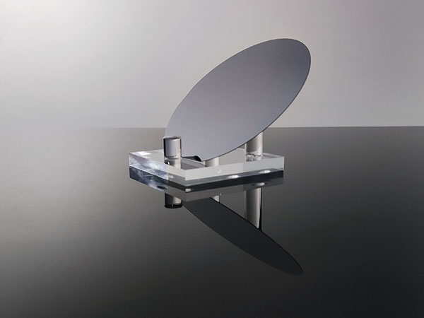
Epitaxial growth of a silicon atomic layer on a silicon wafer substrate, creating what is commonly known as an epitaxial wafer, offers substantial advantages. In CMOS silicon technology, epitaxial growth (EPI) is a critical process step. Here’s an in-depth look at its key roles and benefits:
1. Enhancing Crystal Quality
Reducing Substrate Defects and Impurities:
During wafer manufacturing, defects and impurities can be introduced into the substrate. By growing an epitaxial layer on the substrate, we create a high-quality single-crystal silicon layer with low defect and impurity concentrations. This epitaxial wafer provides a superior foundation for subsequent device fabrication, ensuring that high-quality material is used to produce high-performance devices.
Uniform Crystal Structure:
Epitaxial growth ensures a more uniform crystal structure, reducing the impact of grain boundaries and crystal defects in the substrate material. This enhancement is essential for manufacturing high-reliability and high-performance semiconductor devices, as the epitaxial wafer exhibits consistent and superior crystal quality across its entire surface.
2. Improving Electrical Properties
Optimizing Device Electrical Characteristics:
The epitaxial wafer allows for precise control over the silicon’s doping concentration and type, optimizing the electrical properties of devices. For instance, the epitaxial layer’s doping levels can be finely adjusted to control the threshold voltage of MOSFETs and other critical electrical parameters, tailored to specific application needs.
Reducing Leakage Current:
The high-quality epitaxial layer within the epitaxial wafer has a lower defect density, which helps to reduce leakage current in devices. This improvement enhances device performance and significantly boosts reliability and longevity, making the epitaxial wafer an essential component for advanced semiconductor devices.

(GaAs Epitaxial Wafer)
3. Supporting Advanced Process Nodes
Scaling Down Feature Sizes:
As process nodes continue to shrink (e.g., 7nm, 5nm), the precision and quality requirements for materials become increasingly stringent. Epitaxial growth technology meets these demands, supporting the production of high-performance and high-density integrated circuits. The epitaxial wafer, with its precise material properties, enables the scaling down of feature sizes critical for next-generation semiconductor devices.
Increasing Breakdown Voltage:
The epitaxial layer can be engineered to have a higher breakdown voltage, which is crucial for manufacturing high-power and high-voltage devices. For instance, in power semiconductor devices, the high breakdown voltage characteristic of the epitaxial wafer significantly enhances the device's safe operating range and overall performance, providing a robust solution for demanding applications.
4. Enabling Process Compatibility and Multi-Layer Structures
Fabricating Multi-Layer Structures:
Epitaxial growth technology allows the creation of multi-layer structures on the substrate. Different layers can have varying doping concentrations and types, providing flexibility in device design. This capability is particularly beneficial for fabricating complex CMOS devices and three-dimensional integration technologies, where the epitaxial wafer’s multi-layer configuration offers significant design and performance advantages.
High Compatibility with Existing Processes:
The epitaxial growth process is highly compatible with current CMOS manufacturing processes. It integrates seamlessly into existing production workflows without significant modifications to the process line, reducing costs and accelerating the deployment of new technologies. This compatibility makes the epitaxial wafer an efficient and effective solution in modern semiconductor manufacturing.
Summary
In CMOS silicon technology, the application of epitaxial growth primarily aims to enhance the crystal quality of wafers, optimize device electrical performance, support advanced process nodes, and meet the demands for high-performance and high-density integrated circuits. The epitaxial wafer, with its precisely controlled doping and structure, significantly improves the overall performance and reliability of semiconductor devices. These advantages make epitaxial growth an indispensable process in the manufacture of modern epitaxial wafers for semiconductor applications.
For those seeking high-quality epitaxial wafers, JXT stands out as a premier provider. JXT offers superior epitaxial wafers that meet the exacting standards of today's advanced semiconductor industry. With a commitment to quality and precision, JXT's epitaxial wafers are designed to enhance device performance and reliability across a wide range of applications.
As semiconductor technology advances, Gallium Nitride (GaN) has become a core material in optoelectronics, rad...
With the rapid advancement of third-generation semiconductor technologies, Silicon Carbide (SiC) has emerged a...
As third-generation semiconductor materials such as silicon carbide (SiC) and gallium nitride (GaN) continue t...
