SiC is a binary compound formed by Si and C elements in a 1:1 ratio, i.e., 50% Si and 50% C, with its basic structural unit being a Si-C tetrahedron.
For example, Si atom diameter is larger, equivalent to an apple, while C atom diameter is smaller, equivalent to an orange. When an equal number of oranges and apples are stacked together, a SiC crystal is formed.
SiC is a binary compound where the Si-Si bond atomic spacing is 3.89 A. How should this spacing be understood? The most advanced lithography machine on the market today has a lithography precision of 3nm, which is 30A in distance. The lithography precision is 8 times the atomic distance.
The Si-Si bond energy is 310 kJ/mol, which can be understood as the force required to separate these two atoms. The larger the bond energy, the greater the force required to separate the atoms.
The Si-C bond atomic spacing is 1.89 A, and the bond energy is 447 kJ/mol.
From the bond energy, it can be seen that compared to traditional silicon-based semiconductor materials, SiC-based semiconductor materials have more stable chemical properties.

From the figure, it can be seen that any one C atom is bonded to the four nearest Si atoms, while any one Si atom is bonded to the four nearest C atoms. The SiC crystal structure can also be described using a layered structure method, as shown in the figure, where several C atoms occupy the hexagonal lattice points in the same plane, forming a C-atom close-packed layer, and Si atoms also occupy the hexagonal lattice points in the same plane and form a Si-atom close-packed layer.
Each C atom in the C-atom close-packed layer is connected to the nearest Si atom, and the same is true for the Si-atom close-packed layer. Each pair of adjacent C and Si atom close-packed layers forms a carbon-silicon dual-atom layer.
The arrangement of SiC crystals is very rich, and over 200 SiC crystal types have been discovered so far.
This is similar to the game of Tetris, where the smallest unit blocks are all the same, but when the blocks are combined together, they form different shapes.
The spatial structure of SiC is slightly more complex than Tetris, with its smallest unit changing from a small square to a small tetrahedron made up of C atoms and Si atoms.
To distinguish between different types of SiC, the Ramsdell method is currently mainly used for marking. This method uses a combination of letters and numbers to represent the different types of SiC.
The letter is placed behind, used to indicate the type of crystal cell. C represents the cubic crystal type (the first letter of Cubic in English), H represents the hexagonal crystal type (the first letter of Hexagonal in English), and R represents the rhombic crystal type (the first letter of Rhombus in English). The digits are placed in front to indicate the number of Si-C double atomic layers in the basic repeating unit.
Except for 2H-SiC and 3C-SiC, other crystal structures can be considered as a mixture of zinc blende and wurtzite structures, which is also a close-packed hexagonal structure.
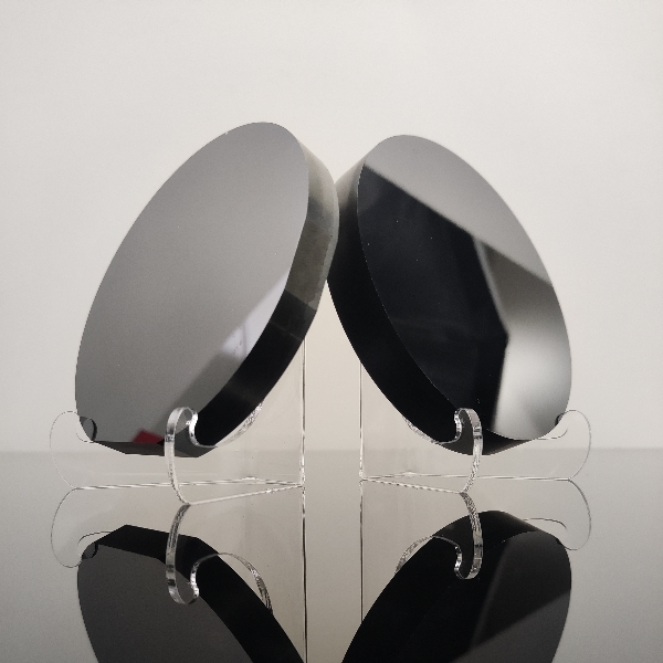
The C-face refers to the (000-1) crystal face of the silicon carbide wafer, which is the surface of the crystal cut along the negative c-axis direction, and the terminating atom on this surface is a carbon atom.
The silicon face refers to the (0001) crystal face of the silicon carbide wafer, which is the surface of the crystal cut along the positive c-axis direction, and the terminating atom on this surface is a silicon atom.
The difference between the C-face and the silicon face will affect the physical and electrical properties of the silicon carbide wafer, such as thermal conductivity, electrical conductivity, carrier mobility, and interface state density.
The choice of the C-face or the silicon face will also affect the manufacturing process and performance of the silicon carbide device, such as epitaxial growth, ion implantation, oxidation, metal deposition, and contact resistance.
As semiconductor technology advances, Gallium Nitride (GaN) has become a core material in optoelectronics, rad...
With the rapid advancement of third-generation semiconductor technologies, Silicon Carbide (SiC) has emerged a...
As third-generation semiconductor materials such as silicon carbide (SiC) and gallium nitride (GaN) continue t...