In the semiconductor industry, Semiconductor wafer quality assessment is critical for ensuring the performance and reliability of devices. Understanding and evaluating various parameters is essential for maintaining high standards. Below are some key terms and their significance in wafer quality assessment:
1. Crystal Orientation: This refers to the crystallographic direction in which the wafer is cut, typically denoted by Miller indices (e.g., <100>, <111>). Different orientations affect the crystal's mechanical strength, electron mobility, and other physical properties.
2. Conductivity Type: The type of electrical conductivity in a silicon wafer, classified as n-type (where electrons are the majority carriers) or p-type (where holes are the majority carriers). Conductivity type is determined by doping the silicon with specific elements, such as phosphorus for n-type and boron for p-type.
3. Dopant Impurities: Elements intentionally introduced into the crystal to control its electrical properties. For instance, phosphorus doping results in n-type silicon, while boron doping results in p-type silicon. The type and concentration of dopants significantly influence the wafer's electrical behavior.
4. Resistivity: The resistance of the material to electric current flow, typically measured in ohm-centimeters (Ω·cm). Resistivity is influenced by the concentration of dopants and the presence of crystal defects.
5. Rocking Curve Full Width at Half Maximum (FWHM): The width of the X-ray rocking curve at half its maximum intensity, used to assess the crystal lattice's integrity and strain state. A narrower FWHM indicates higher crystal quality.
6. Dislocation Density: The number of dislocations per unit area within the crystal. High dislocation density usually indicates a greater number of defects, which can adversely affect the performance and reliability of semiconductor devices.
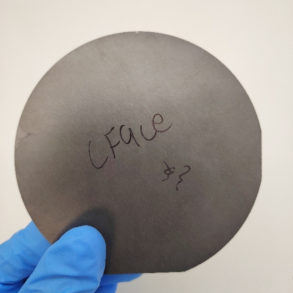
7. Dimension: The wafer's diameter and thickness. Common wafer diameters include 150mm, 200mm, and 300mm. Accurate dimensions are crucial for compatibility with manufacturing processes.
8. Surface Polishing: The process of making the wafer surface smooth and flat through mechanical or chemical means. The quality of surface polishing directly impacts the wafer's surface roughness and flatness, which are critical for subsequent fabrication steps.
9. Surface Roughness: The microscopic unevenness of the wafer surface, often quantified by root mean square (RMS) or peak-to-valley (Ra) measurements. Lower surface roughness is essential for enhancing device performance and yield.
10. Flatness: The macroscopic flatness of the wafer surface, usually measured by total thickness variation (TTV) or waviness. High flatness ensures precision in photolithography and etching processes.

These terms encompass a broad spectrum of attributes, from physical dimensions and surface characteristics to internal structure. They serve as vital indicators in evaluating wafer quality, ensuring that the wafers meet the stringent requirements of semiconductor device manufacturing. Understanding these parameters helps in maintaining the high standards necessary for producing reliable and high-performance electronic components.
Related product links
Silicon Carbide Wafer (SiC Wafer)
As semiconductor technology advances, Gallium Nitride (GaN) has become a core material in optoelectronics, rad...
With the rapid advancement of third-generation semiconductor technologies, Silicon Carbide (SiC) has emerged a...
As third-generation semiconductor materials such as silicon carbide (SiC) and gallium nitride (GaN) continue t...