Silicon epitaxial layers and substrates are two important components in the semiconductor manufacturing process. The substrate is the basis for semiconductor chip manufacturing and is mainly made of single crystal silicon material. The silicon epitaxial layer is a layer of silicon material processed and grown on the substrate, and its material properties are the same as the substrate. Both are different in composition, structure and properties.
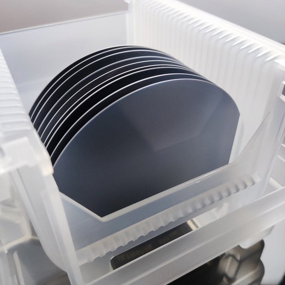
Substrate, as a wafer made of semiconductor single crystal material, can either directly enter the wafer manufacturing process and be used to produce semiconductor devices; it can also be processed through epitaxial processes to produce epitaxial wafers. The semiconductor substrate is like a "foundation" that supports the entire semiconductor structure and ensures that it will not crack or be damaged. At the same time, the substrate itself also has some special electrical, optical and mechanical properties, which are crucial to the performance of semiconductors.
If an integrated circuit is compared to a high-rise building, then the substrate is undoubtedly the solid foundation. In order to ensure their supporting role, these materials must show a high degree of consistency in their crystal structure. Just like high-purity single crystal silicon, its purity and perfection are the cornerstones of building a solid foundation. Only when the foundation is solid and reliable can the stability and perfection of the building above be ensured. Simply put, without the right substrate, we cannot build stable and well-performing semiconductor devices.

Epitaxy
Epitaxy refers to the process of accurately growing a new layer of single crystal on a carefully cut and polished single crystal substrate. This new single crystal can be made of the same material as the substrate (homoepitaxial) or different (heteroepitaxial). Because the new single crystal layer strictly follows the crystalline phase of the substrate and grows, it is called an epitaxial layer, and its thickness is usually controlled at the level of a few microns. Taking silicon as an example, epitaxial growth is to form a layer of new crystals with the same crystal orientation, different resistivities and thicknesses, and a complete lattice structure on a silicon single crystal substrate with a specific crystal orientation. The epitaxially grown substrate is called an epitaxial wafer. Its core value lies in the epitaxial layer, and device production revolves around this layer.
The value of epitaxial wafers is reflected in their ingenious combination of materials. For example, by growing a thin layer of GaN epitaxy on a lower-cost silicon wafer, it is possible to partially realize the wide bandgap characteristics of expensive and excellent third-generation semiconductors using relatively inexpensive first-generation semiconductor materials. , achieving high cost performance. However, heteroepitaxial structures are also accompanied by a series of challenges, such as lattice mismatch, inconsistent temperature coefficients and poor thermal conductivity. Just like building scaffolding on a plastic foundation, different materials will have differences in expansion and contraction when the temperature changes, and Silicon's thermal conductivity is not ideal.
Homoepitaxy, that is, growing an epitaxial layer that is the same as the substrate material on the substrate, is meant to further improve the stability and reliability of the product. Although the materials are the same, the material purity and uniformity on the wafer surface are significantly improved through epitaxy processing. Compared with mechanically polished polished wafers, the surface of epitaxial wafers is smoother and cleaner, with significantly reduced micro-defects and impurities, more uniform resistivity, and more precise control of defects such as surface particles, stacking faults, and dislocations. Therefore, epitaxy technology not only optimizes product performance, but also ensures product stability and reliability.
In the fields of modern electronics, optoelectronics, microelectronics and information technology, semiconductor substrates and epitaxial technologies play an indispensable role. They provide a solid foundation for manufacturing high-performance, high-reliability semiconductor devices. With the continuous development of science and technology, semiconductor substrate and epitaxial technology will also continue to advance, bringing new breakthroughs and developments to the future semiconductor industry.
As semiconductor technology advances, Gallium Nitride (GaN) has become a core material in optoelectronics, rad...
With the rapid advancement of third-generation semiconductor technologies, Silicon Carbide (SiC) has emerged a...
As third-generation semiconductor materials such as silicon carbide (SiC) and gallium nitride (GaN) continue t...