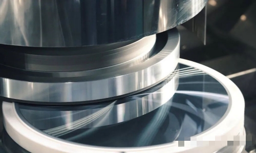
As modern electronic devices evolve towards miniaturization, thinness, and high performance, integrated circuit (IC) manufacturing processes are continuously optimized to meet increasingly stringent technical demands. Wafer thinning, a critical step in the back-end processing of IC manufacturing, plays a significant role in enhancing packaging performance, heat dissipation, and overall production efficiency. This article will explore the importance of wafer thinning in contemporary semiconductor manufacturing, discussing its benefits from the perspectives of packaging requirements, thermal performance, and cost control, while incorporating the specific thickness characteristics of silicon carbide (SiC) wafers.
1. Meeting Packaging Requirements
The thickness of the wafer has a direct impact on the size and performance of IC packages. For instance, the standard thickness of silicon carbide wafers varies depending on their diameter, with typical values as follows:
2-inch (50.8 mm) wafers: 350 µm – 500 µm
3-inch (76.2 mm) wafers: 350 µm – 600 µm
4-inch (100 mm) wafers: 400 µm – 650 µm
6-inch (150 mm) wafers: 500 µm – 1,000 µm
8-inch (200 mm) wafers: 700 µm – 1,000 µm
While these thicknesses are adequate for early-stage processes such as lithography and etching, where mechanical strength is essential to ensure stable handling within and between equipment, they are often too thick for the packaging stage. To achieve compact device designs, wafers typically need to be thinned to a range of 100 µm to 200 µm, or even thinner. Thinning the wafer significantly reduces the overall package height, making it more suitable for space-constrained designs. This not only facilitates the miniaturization of electronic products but also provides additional internal space for more complex circuitry and components, thereby enhancing the device's integration and overall performance.
2. Enhancing Packaging Process Operability
Wafer thinning also plays an important role in key packaging processes, such as wire bonding. During wire bonding, the distance between the electrodes on the chip and the package leads determines the length of the bonding wires. After thinning, this distance is reduced, which shortens the bonding wires, thereby minimizing signal transmission delay and energy loss. This improvement directly enhances the chip's signal transmission performance and reliability.
Moreover, wafer thinning is a prerequisite for advanced packaging techniques such as wafer-level packaging (WLP) and three-dimensional (3D) packaging. Through thinning, wafers can more easily adapt to these high-density packaging technologies, improving integration while reducing material and manufacturing costs. Therefore, wafer thinning not only optimizes packaging process efficiency but also supports innovation in packaging design.

3. Improving Thermal Performance
Integrated circuits generate significant heat during operation, especially in high-power applications such as servers and graphics processing units (GPUs), where effective heat management is critical to maintaining performance and reliability. Wafer thinning significantly improves the chip's thermal performance by reducing its thermal resistance, thus increasing heat conduction efficiency.
In the case of silicon carbide wafers, known for their excellent thermal conductivity, thinning further enhances their heat dissipation capabilities. A thinner wafer allows heat to be conducted more quickly to the chip's surface, lowering the operating temperature and improving the stability and reliability of the device. Furthermore, thinning provides more options for thermal management design, such as directly attaching heat sinks or thermal pipes to the back of the chip, ensuring efficient heat dissipation. This is particularly critical in applications that demand high thermal efficiency, such as aerospace and military equipment.
4. Reducing Manufacturing Costs
In addition to improving chip performance, wafer thinning offers significant cost advantages. By reducing wafer thickness, the consumption of semiconductor materials—such as silicon carbide, which is relatively expensive—can be minimized. Thinning allows more chips to be produced from a single wafer, thereby lowering the material cost per chip.
Additionally, thinner wafers save space during packaging, transportation, and storage, further reducing logistics and storage costs. Meanwhile, in manufacturing processes like lithography and etching, thinner wafers result in reduced light scattering, improving precision and process efficiency. This not only enhances the accuracy of the manufacturing process but also shortens production cycles, leading to increased overall production efficiency and cost savings.
5. Increasing Production Efficiency
Wafer thinning plays a crucial role in boosting production efficiency. Thinner wafers are easier to handle during packaging and testing, reducing processing time. Moreover, thinning simplifies certain manufacturing steps, making the entire process more efficient. As production efficiency improves, chip manufacturers can complete production in a shorter time frame, reducing time to market and enhancing competitiveness.
Conclusion
Wafer thinning is indispensable in integrated circuit manufacturing, especially as electronic devices trend towards smaller, thinner designs. Using silicon carbide wafers as an example, their standard thicknesses provide sufficient mechanical strength during early-stage processing, but must be thinned during packaging to meet thickness requirements, improve thermal performance, and reduce manufacturing costs. Thinning not only enables chip miniaturization and enhances packaging and thermal capabilities but also leads to significant cost reductions and production efficiency gains. As semiconductor technology continues to advance, wafer thinning will remain a critical process in enabling cutting-edge packaging techniques, driving innovation and growth in the integrated circuit industry.
As semiconductor technology advances, Gallium Nitride (GaN) has become a core material in optoelectronics, rad...
With the rapid advancement of third-generation semiconductor technologies, Silicon Carbide (SiC) has emerged a...
As third-generation semiconductor materials such as silicon carbide (SiC) and gallium nitride (GaN) continue t...
