Recently, a renowned international client conducted a thorough evaluation of JXT's 4H Silicon Carbide (SiC) wafers and provided detailed technical feedback. The client assessed key aspects such as transmission, reflection, and overall crystalline quality, verifying the superiority of JXT's 4H-HPSI SiC material through experimental data. Below, we will present a technical overview of JXT's SiC products, incorporating the provided test graphs to highlight their unique properties and competitive advantages.
Material Transparency and Optical Performance
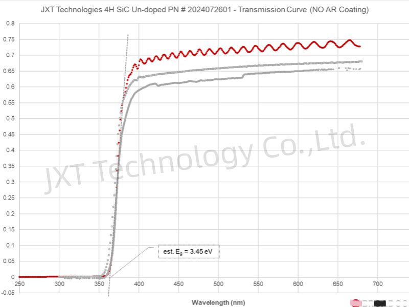
The transmission curve (see Figure 1) provided by the client clearly demonstrates the excellent transmission performance of JXT’s 4H-HPSI SiC wafer across the 250 nm to 750 nm wavelength range. The data shows a rapid increase in transmission after 350 nm, eventually stabilizing at around 70% beyond 400 nm. This high level of transmission in the visible spectrum (VIS) suggests a very low density of point defects in the material, which is crucial for applications in optoelectronics and high-power devices. The superior transparency ensures higher efficiency and performance in devices where light transmission is a key factor.

Figure 1
Crystalline Quality and Reflection Performance
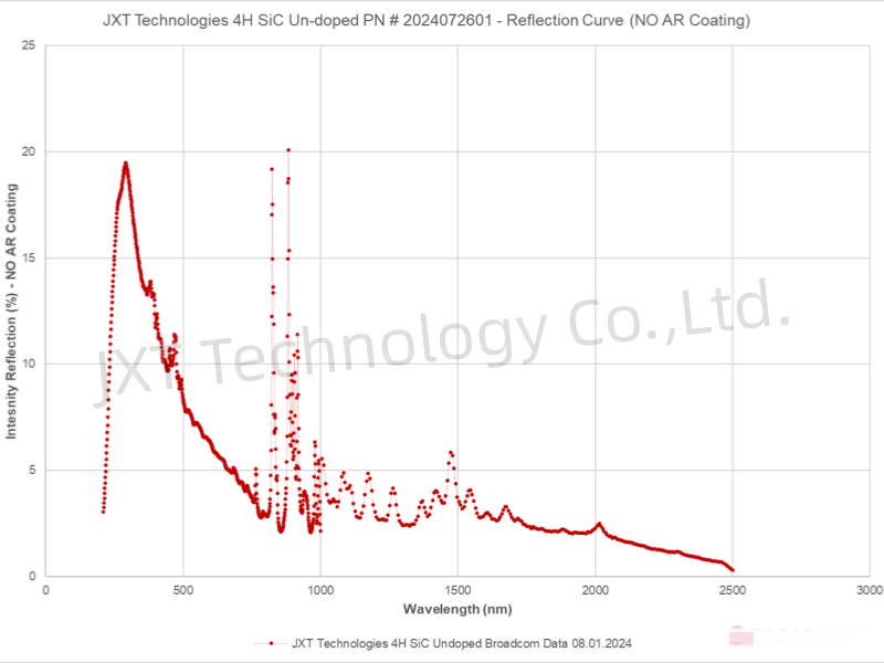
The reflection curve (see Figure 2) illustrates the reflection characteristics of JXT’s 4H-HPSI SiC wafer measured across a wavelength range from 300 nm to 2500 nm. The reflection peaks near 20% at around 400 nm before dropping significantly, and stabilizes between 2% and 5% in the 1500 nm to 2500 nm range. This indicates the material’s excellent optical performance over a wide range of wavelengths, making it highly suitable for optical device applications that require minimal reflection and enhanced light management.

Figure 2
Point Defect Control and Material Quality
The client’s report emphasizes that the low density of point defects in JXT’s 4H-HPSI SiC material significantly enhances its transparency and optical properties. The reduction in point defects not only minimizes optical scattering and absorption but also improves the overall stability and uniformity of the wafers. In high-power and high-frequency electronic applications, the low defect density plays a critical role in ensuring the long-term performance and reliability of the devices.
Competitive Comparison
As shown in the transmission curve (Figure 1), JXT's 4H-HPSI SiC wafer demonstrates superior performance compared to other vendors' V-doped semi-insulating SiC substrates. Within the 350 nm to 750 nm wavelength range, JXT's product exhibits significantly higher transmission rates, underscoring its exceptional optical transparency. This makes it a highly promising candidate for optoelectronic applications requiring advanced material properties.
Key Advantages of JXT’s SiC Products
High Transparency and Low Defect Density: The outstanding transmission in the visible spectrum underscores the material's suitability for a wide range of optoelectronic applications.
Superior Crystalline Quality: The low point defect density ensures excellent performance in high-temperature and high-frequency environments.
Reliability and Consistency: The client’s test results confirm that JXT’s SiC wafers meet industry standards across various technical parameters, laying a strong foundation for future collaborations.
Conclusion
The test data and graphical analysis provided by the client highlight JXT’s 4H-HPSI SiC wafers as a standout product in terms of optical transparency, reflection performance, and overall material quality. The wafer's high transmission and low reflection rates across a wide wavelength range make it ideal for use in optoelectronic devices. Moreover, when compared to other products on the market, JXT’s SiC wafers clearly outperform in terms of key metrics, making them an excellent choice for future high-power semiconductor and optoelectronic device applications.
The promising results of this evaluation reaffirm JXT’s position as a leading supplier of high-quality SiC materials, poised to meet the growing demands of the semiconductor and power electronics industries.
As semiconductor technology advances, Gallium Nitride (GaN) has become a core material in optoelectronics, rad...
With the rapid advancement of third-generation semiconductor technologies, Silicon Carbide (SiC) has emerged a...
As third-generation semiconductor materials such as silicon carbide (SiC) and gallium nitride (GaN) continue t...
