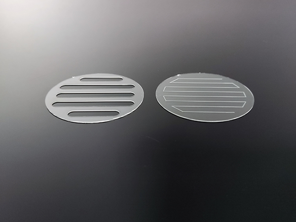
Silicon carbide (SiC), as a third-generation semiconductor material, plays a crucial role in modern high-tech applications due to its wide bandgap, high thermal conductivity, excellent chemical stability, and radiation resistance. Particularly, 2-inch, 3-millimeter thick silicon carbide substrates find extensive use in various advanced technology sectors, with their unique physical and chemical properties making them ideal for manufacturing numerous advanced devices. This article explores the key applications of these substrates and introduces the custom processing services offered by JXT.
1. Applications in Power Electronic Devices
Silicon carbide substrates are particularly valued in the field of power electronics due to their high breakdown voltage and high electron saturation velocity. Compared to traditional silicon-based materials, SiC-based devices can significantly enhance operational efficiency and power density while reducing power consumption. Common applications include:
Silicon Carbide Schottky Diodes: These diodes exhibit outstanding efficiency and fast response characteristics in high-frequency switch mode power supplies, electric vehicle chargers, and inverters. The low forward voltage drop and low switching losses associated with silicon carbide diodes make them key components in the next generation of efficient power conversion equipment.
SiC MOSFETs: Silicon carbide MOSFETs, known for their exceptional performance in high voltage and high-temperature environments, are widely used in solar inverter systems, electric vehicle power modules, and industrial power management systems. SiC MOSFETs can significantly reduce energy losses compared to traditional silicon-based MOSFETs, enhancing energy conversion efficiency.
2. High-Frequency and High-Temperature Electronic Devices
The wide bandgap characteristics of silicon carbide materials provide unparalleled advantages in high-temperature and high-frequency applications. In sectors such as 5G communications, aerospace, and automotive electronics, the use of silicon carbide substrates is becoming increasingly prevalent:
RF Power Amplifiers: The high electron mobility and high breakdown voltage of silicon carbide enable RF power amplifiers based on SiC to operate efficiently at high power and frequency, making them suitable for high-frequency communication scenarios such as 5G base stations and satellite communication equipment.
High-Temperature Sensors: SiC substrates exhibit extreme thermal stability, making them ideal for use in high-temperature environments, such as monitoring sensors for automotive engines and oil exploration equipment. Silicon carbide sensors can operate reliably in temperatures exceeding 600°C, ensuring data integrity in extreme conditions.
3. Applications in Optoelectronic Devices
Silicon carbide materials are not only used in power devices but also show significant promise in the optoelectronic field, particularly as substrates for gallium nitride (GaN) materials, widely applied in LED and laser devices:
LED Lighting: As an ideal choice for gallium nitride epitaxial materials, silicon carbide substrates enhance the luminous efficiency and power density of LEDs, particularly in high-brightness LEDs and solid-state lighting applications. SiC-based LED light sources are widely used in automotive headlights, display screens, and general lighting.
Blue and Violet Lasers: SiC substrates also play a vital role in blue and violet laser devices, which are commonly used in high-density optical storage, optical disc drives, and high-precision projection systems.
4. Power Conversion and Inverters
The high voltage tolerance and low switching losses of SiC substrates make them indispensable in power conversion and inverter applications. In sectors such as solar power generation, wind energy, and electric vehicles, SiC-based devices can significantly enhance energy conversion efficiency:
Power Converters: Power converters using silicon carbide substrates find extensive applications in electric vehicle charging stations and solar photovoltaic inverters. These devices can withstand high voltages and provide faster switching speeds, thereby reducing power losses and improving overall energy utilization.
5. Microelectromechanical Systems (MEMS)
The high mechanical strength and corrosion resistance of silicon carbide materials make them widely applicable in extreme environments, particularly suitable for use in microelectromechanical systems (MEMS). SiC MEMS devices offer stable performance in harsh conditions:
High-Temperature Pressure Sensors: Silicon carbide substrates are ideal for manufacturing pressure sensors capable of operating in high-temperature environments, commonly used in oil drilling and aerospace sectors for extreme environmental monitoring.
JXT's Custom Processing Services for Silicon Carbide Wafers
As a professional crystal materials supplier, JXT is able to provide high-quality silicon carbide wafers covering a range of sizes from 2 inches to 8 inches. In addition to standard specifications, JXT also offers custom processing services to meet the specific needs of customers in various industries. JXT's custom processing services include:
Multiple Size Options: Availability of silicon carbide wafers in sizes ranging from 2 inches to 8 inches based on customer requirements.
Thickness Customization: Thickness options ranging from hundreds of microns to several millimeters, suitable for different application scenarios such as power devices and optoelectronic devices.
Multiple Crystal Orientation Options: JXT's silicon carbide substrates support both conductive and semi-insulating materials, meeting diverse needs across various fields.
Laser Cutting Services: JXT also provides precision laser cutting services for silicon carbide wafers, enabling the customization of substrates or devices into different shapes as per customer specifications, with high processing accuracy and efficiency.
Through these flexible custom options, JXT ensures the provision of the most suitable silicon carbide substrate solutions for customers, meeting diverse technical requirements across various applications, and promoting advancements in the semiconductor, power electronics, and optoelectronic industries.

Conclusion
The 2-inch, 3-millimeter thick silicon carbide substrates, due to their excellent physical properties, play a significant role in power electronics, high-frequency communications, optoelectronics, and extreme environment sensors. The high-quality silicon carbide substrates and customized processing services provided by JXT can meet the specific needs of customers in various sectors, facilitating technological innovation and development.
As semiconductor technology advances, Gallium Nitride (GaN) has become a core material in optoelectronics, rad...
With the rapid advancement of third-generation semiconductor technologies, Silicon Carbide (SiC) has emerged a...
As third-generation semiconductor materials such as silicon carbide (SiC) and gallium nitride (GaN) continue t...
