Silicon carbide (SiC) is a crucial wide-bandgap semiconductor material widely used in high-power electronics and optical devices. Depending on the application requirements, SiC wafers are typically categorized into conductive and semi-insulating types. Conductive SiC wafers are doped with conductive impurities, such as nitrogen or phosphorus, to enhance their electrical conductivity. In contrast, semi-insulating SiC wafers undergo specific processing to achieve high resistivity, making them suitable for use in optical, RF, and microwave devices. This article compares and analyzes the transmittance characteristics of conductive and semi-insulating SiC wafers under visible light, providing insights into their optical performance for various applications.
Overview of Transmittance Testing
The transmittance of both types of SiC wafers was studied across a wavelength range from 190 nm to 1100 nm using spectroscopic analysis. The results show significant differences in transmittance between the two types of wafers, especially in the visible light spectrum (400-700 nm), where the optical properties of the materials vary notably.
Transmittance Analysis of Semi-Insulating SiC Wafers
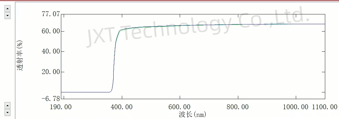
As shown in Figure 1, the transmittance curve of the semi-insulating SiC wafer rises sharply around 400 nm and stabilizes at approximately 60%. The wafer maintains this high transmittance throughout the visible light range (400-700 nm). This characteristic is largely due to the intrinsic properties of semi-insulating SiC, which, being free of free carriers, experiences minimal absorption during light transmission, thus enabling high transparency.

This high transparency makes semi-insulating SiC ideal for use in optical devices, particularly where high transmittance is required. For instance, it is commonly used in photodetectors and optical communication systems, where its high transparency can significantly enhance the efficiency of light signal transmission.
Transmittance Analysis of Conductive SiC Wafers
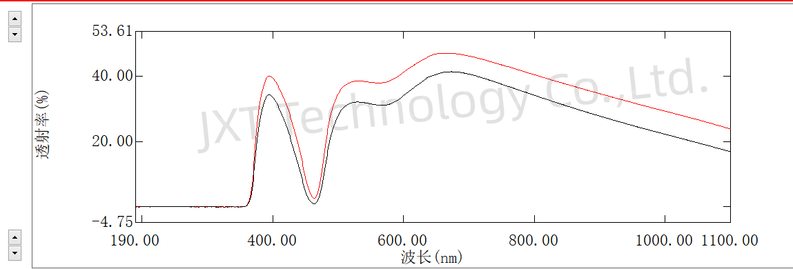
In contrast, Figure 2 illustrates the transmittance behavior of conductive SiC wafers, which exhibit considerable oscillation across the spectrum. Notably, in the visible light range, the transmittance falls below 40%, with a pronounced absorption dip occurring around 500 nm. This behavior can be attributed to free carrier absorption in the conductive SiC, where the doped impurities interact with light, leading to energy absorption and reduced transmittance.

Additionally, the oscillations in transmittance at different wavelengths may be due to interference effects, as well as factors such as wafer thickness and refractive index. These interference effects can result in periodic fluctuations in light transmittance, leading to peaks and troughs at specific wavelengths. Given the lower transmittance and significant oscillations, conductive SiC wafers are more suitable for high-power electronic devices rather than high-transparency optical applications.
Comparative Analysis
By comparing the optical performance of conductive and semi-insulating SiC wafers, several conclusions can be drawn:
Transmittance Levels: Semi-insulating SiC wafers exhibit significantly higher transmittance across the visible spectrum compared to conductive SiC wafers. The transmittance of semi-insulating SiC approaches 60%, while that of conductive SiC remains below 40% in the same wavelength range.
Absorption Characteristics: Conductive SiC wafers, due to their internal free carriers, show enhanced absorption in the visible light range, with a prominent absorption dip around 500 nm. In contrast, semi-insulating SiC experiences minimal additional absorption.
Application Differences: Semi-insulating SiC wafers, with their high transparency, are well-suited for optical devices and sensors that require high transmittance. On the other hand, conductive SiC wafers are commonly used in power electronic devices due to their superior electrical conductivity.
Conclusion
The transmittance characteristics of conductive and semi-insulating SiC wafers under visible light differ significantly. Semi-insulating SiC wafers, with their lower free carrier density, exhibit high transmittance in the visible light spectrum, making them ideal for optical applications. In contrast, conductive SiC wafers show lower transmittance and greater oscillation, which are mainly due to the presence of doped impurities and related absorption effects, making them more suitable for power electronics. When selecting a type of SiC wafer for practical applications, one should consider the specific optical and electrical properties of each type and align them with the application's requirements.
As semiconductor technology advances, Gallium Nitride (GaN) has become a core material in optoelectronics, rad...
With the rapid advancement of third-generation semiconductor technologies, Silicon Carbide (SiC) has emerged a...
As third-generation semiconductor materials such as silicon carbide (SiC) and gallium nitride (GaN) continue t...
