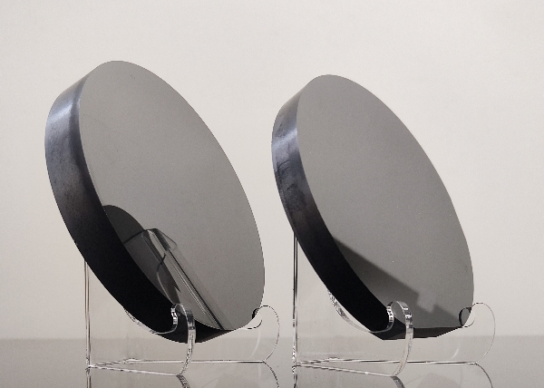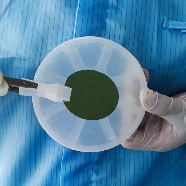
The processing of 4H-SiC substrates involves the following key steps:
1. Crystal Orientation: X-ray diffraction (XRD) is used to orient the ingot. When an X-ray beam is directed at the crystal plane to be oriented, the crystal orientation is determined by the angle of the diffracted beams.
2. Outer Diameter Grinding: Single crystals grown in graphite crucibles often exceed the standard diameter. Outer diameter grinding is used to reduce the crystal diameter to the standard size.
3. End Face Grinding: Typically, 4-inch 4H-SiC substrates have two alignment edges: the primary and secondary flat. These edges are created using end face grinding.

4. Wire Sawing: Wire sawing is a crucial step in the processing of 4H-SiC substrates. Damage such as cracks and subsurface damage caused during wire sawing can adversely affect subsequent processing steps. This can extend processing times and lead to wafer loss. The most commonly used wire sawing method for silicon carbide involves a reciprocating diamond wire. This technique uses a metal wire bonded with diamond abrasives that moves back and forth to cut the 4H-SiC ingot. The resulting wafers are typically around 500 μm thick and exhibit significant sawing marks and deep subsurface damage.
5. Edge Chamfering: To prevent edge chipping and cracking during subsequent processes and to reduce wear on grinding and polishing pads, the sharp edges of the wafers are chamfered into specified shapes after wire sawing.
6. Thinning: The wire sawing process leaves numerous scratches and subsurface damage on the wafer surface. Thinning is performed using diamond wheels to feed and remove these imperfections as much as possible.
7. Grinding: Grinding involves both coarse and fine grinding steps, similar to thinning but with finer grit sizes of boron carbide or diamond abrasives. This process has a lower removal rate and primarily focuses on removing any damage left by the thinning process as well as any new damage introduced.
8. Polishing: Polishing is the final step in 4H-SiC substrate processing and is divided into coarse and fine polishing. During this process, a soft oxide layer is formed on the wafer surface under the influence of polishing slurry. This layer is mechanically removed using alumina or silica abrasives. After polishing, the substrate surface is free from scratches and subsurface damage and has an extremely low surface roughness. Polishing is critical for achieving a super-smooth, damage-free surface on the 4H-SiC substrate.
9. Cleaning: The final step is to remove any residual particles, metals, oxide films, and organic contaminants from the processing steps.

As semiconductor technology advances, Gallium Nitride (GaN) has become a core material in optoelectronics, rad...
With the rapid advancement of third-generation semiconductor technologies, Silicon Carbide (SiC) has emerged a...
As third-generation semiconductor materials such as silicon carbide (SiC) and gallium nitride (GaN) continue t...
