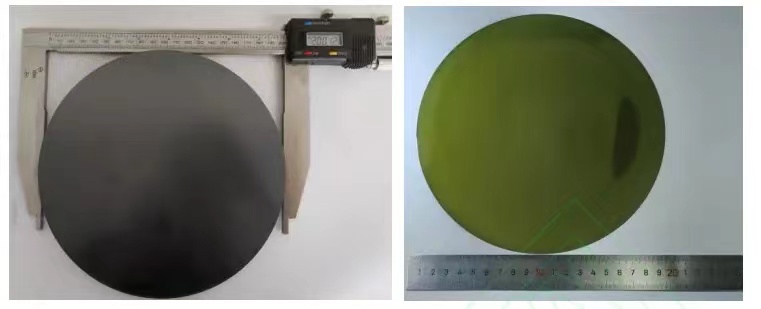
The growth of 8-inch conductive 4H-SiC (Silicon Carbide wafer) wafers is a sophisticated process involving precise techniques and advanced equipment. Below are the main steps and key technologies involved in growing 8-inch conductive 4H-SiC single crystals:
1. Selecting the Appropriate Growth Method
The primary methods for growing 4H-SiC single crystals are Physical Vapor Transport (PVT) and Chemical Vapor Deposition (CVD). Given the requirement for large-size, high-quality crystals, the PVT method is more commonly used.
2. Physical Vapor Transport (PVT) Method
The PVT method involves the sublimation and recondensation of material from a polycrystalline source to form a single crystal. Here are the key steps involved in the PVT process:
Preparation of Equipment:
Crucible: A high-purity graphite crucible is used to contain high-purity SiC powder (the raw material for silicon carbide).
Seed Crystal: A small piece of pre-existing 4H-SiC single crystal, known as the seed crystal, is placed at the top of the crucible.
Heating and Sublimation:
Temperature Control: The entire crucible system is heated to a high temperature, typically between 2000°C and 2500°C.
Sublimation: At these temperatures, the SiC powder sublimates, forming gaseous Si and C atoms or molecules.
Vapor Transport and Recondensation:
Vapor Transport: The Si and C gases move upwards through the crucible due to a temperature gradient inside the system.
Recondensation: Near the seed crystal, the Si and C gases recondense and deposit onto the seed, gradually forming a 4H-SiC single crystal.
Growth Control:
Crystal Growth Rate: The growth rate and quality of the crystal are controlled by adjusting the temperature gradient and gas pressure within the crucible.
Doping Control: By introducing dopants (such as nitrogen or aluminum) in controlled amounts, the electrical type and carrier concentration of the SiC crystal can be tuned.

3. Crystal Processing
The grown SiC single crystal, typically in a cylindrical or disc shape, undergoes further processing:
Slicing: The cylindrical crystal is sliced into thin wafers of the desired thickness.
Grinding and Polishing: The sliced wafers undergo multiple rounds of fine grinding and polishing to ensure smooth and clean surfaces.
Epitaxial Growth: For certain applications, additional layers of SiC are grown on the polished wafers to enhance material performance.
4. Quality Control and Inspection
Quality control is critical throughout the growth and processing stages:
Crystal Structure Inspection: Techniques like X-ray diffraction (XRD) are used to verify that the crystal structure conforms to the characteristics of 4H-SiC.
Defect Analysis: Microscopes and other inspection tools are employed to check for defects in the crystal, such as dislocations and voids.
Electrical Properties Testing: The electrical properties of the crystal, including conductivity, carrier concentration, and mobility, are measured.
Conclusion
The growth process of 8-inch conductive 4H-SiC wafers involves complex physical and chemical processes, including high-temperature sublimation, vapor transport, recondensation, precise growth rate and doping control, and rigorous quality inspection. These steps require sophisticated equipment and highly specialized techniques to produce high-quality SiC single crystals.
As semiconductor technology advances, Gallium Nitride (GaN) has become a core material in optoelectronics, rad...
With the rapid advancement of third-generation semiconductor technologies, Silicon Carbide (SiC) has emerged a...
As third-generation semiconductor materials such as silicon carbide (SiC) and gallium nitride (GaN) continue t...
