Introduction:
Epitaxial technology is a semiconductor fabrication method used to grow crystalline thin films on specific crystal substrates, enabling the fabrication of semiconductor devices with tailored structures and functionalities. Silicon carbide wafer (SiC wafer) and gallium nitride wafers (GaN wafers) are widely studied and applied semiconductor materials that benefit from epitaxial technology. This article will comprehensively analyze the principles, advantages, and applications of epitaxial technology in SiC and GaN wafers.
Epitaxial Technology and its Role:
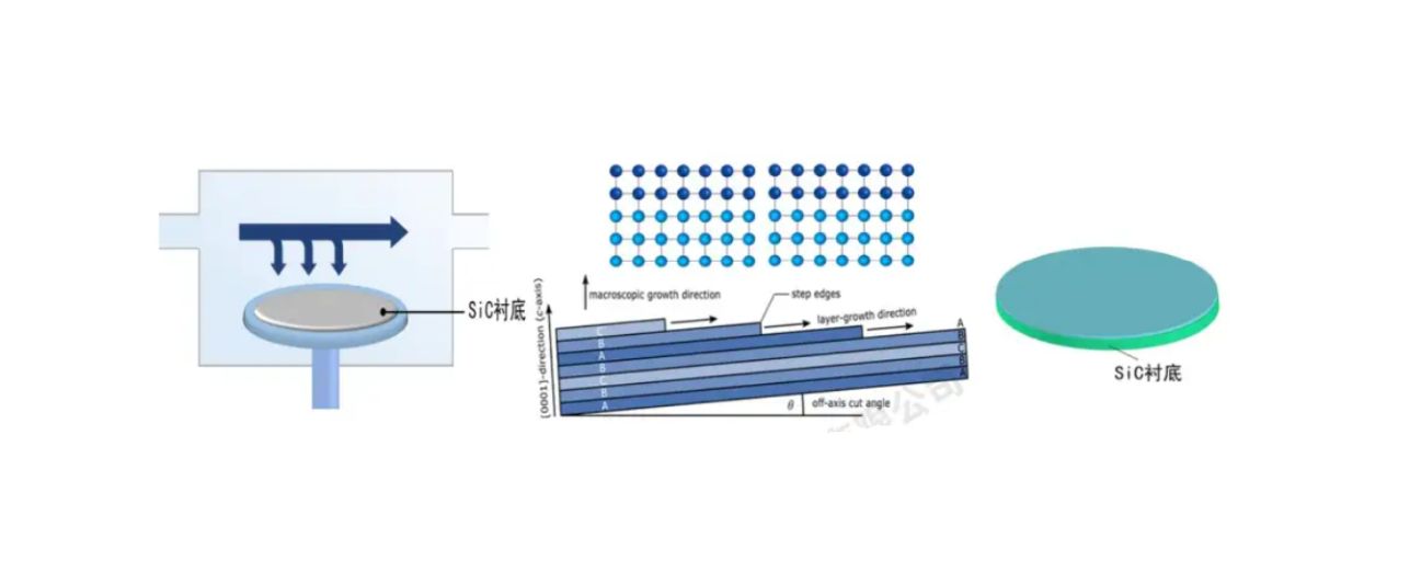
Epitaxial technology involves precisely controlling the growth of crystalline thin films on crystal substrates to achieve desired structures and functionalities. By controlling growth parameters such as temperature, gas flow, and pressure, epitaxial growth conditions can be precisely adjusted, enabling optimization and customization of device performance.

Advantages and Applications of Silicon Carbide Epitaxy:
1. High Thermal Stability: Silicon Carbide wafers exhibit outstanding thermal stability, making them suitable for high-temperature device fabrication, such as high-power power devices.
2. High Electron Mobility: Silicon Carbide wafers feature high electron mobility, suitable for power and high-frequency devices, such as power MOSFETs and Schottky diodes.
3. Wide Bandgap: Silicon Carbide wafers have a wide bandgap, enabling the fabrication of high-power and high-temperature devices, such as power MOSFETs and Schottky diodes.
4. Applications in Optoelectronic Devices: Silicon Carbide epitaxial wafers can be used to fabricate devices such as ultraviolet LEDs and ultraviolet detectors.
Advantages and Applications of Gallium Nitride Epitaxy:
1. Excellent Optoelectronic Performance: Gallium Nitride wafers exhibit excellent optoelectronic performance, suitable for LED lighting, laser diodes, and other optoelectronic devices, such as white LEDs and laser diodes.
2. High-Quality Crystal: Growing Gallium Nitride epitaxy on Gallium Nitride substrates results in high-quality crystal growth, reducing crystal and interface defects and improving device performance and stability.
3. Wide Range of Applications: Gallium Nitride epitaxial wafers can cover a wide spectral range from ultraviolet to infrared, making them suitable for various optoelectronic applications.
Conclusion:
Epitaxial technology plays a crucial role in the fabrication of semiconductor devices using silicon carbide and gallium nitride wafers. Silicon Carbide epitaxy offers advantages such as high thermal stability, high electron mobility, and wide bandgap, suitable for power devices, optoelectronic devices, and high-temperature applications. Gallium Nitride epitaxy, on the other hand, provides excellent optoelectronic performance, high-quality crystal growth, and a wide range of spectral applications, making it suitable for LED lighting, laser diodes, and other optoelectronic applications. By selecting the appropriate epitaxial technology and process conditions, device performance can be optimized to meet diverse application requirements.
As semiconductor technology advances, Gallium Nitride (GaN) has become a core material in optoelectronics, rad...
With the rapid advancement of third-generation semiconductor technologies, Silicon Carbide (SiC) has emerged a...
As third-generation semiconductor materials such as silicon carbide (SiC) and gallium nitride (GaN) continue t...
