Classification of Epitaxial Growth Processes

1、Sapphire crystal growth: Soaking method KY
2、Silicon pulling: Czochralski method CZ (conventional), Floating zone method FZ (high resistance)
3、Gallium arsenide, Indium phosphide, Germanium wafers (the second-generation semiconductors): Vertical gradient freeze method VGF
4、Gallium oxide: Edge-defined film-fed growth method EFG (can be as large as a notebook)
5、Aluminum nitride single crystal: Physical vapor transport method PVT
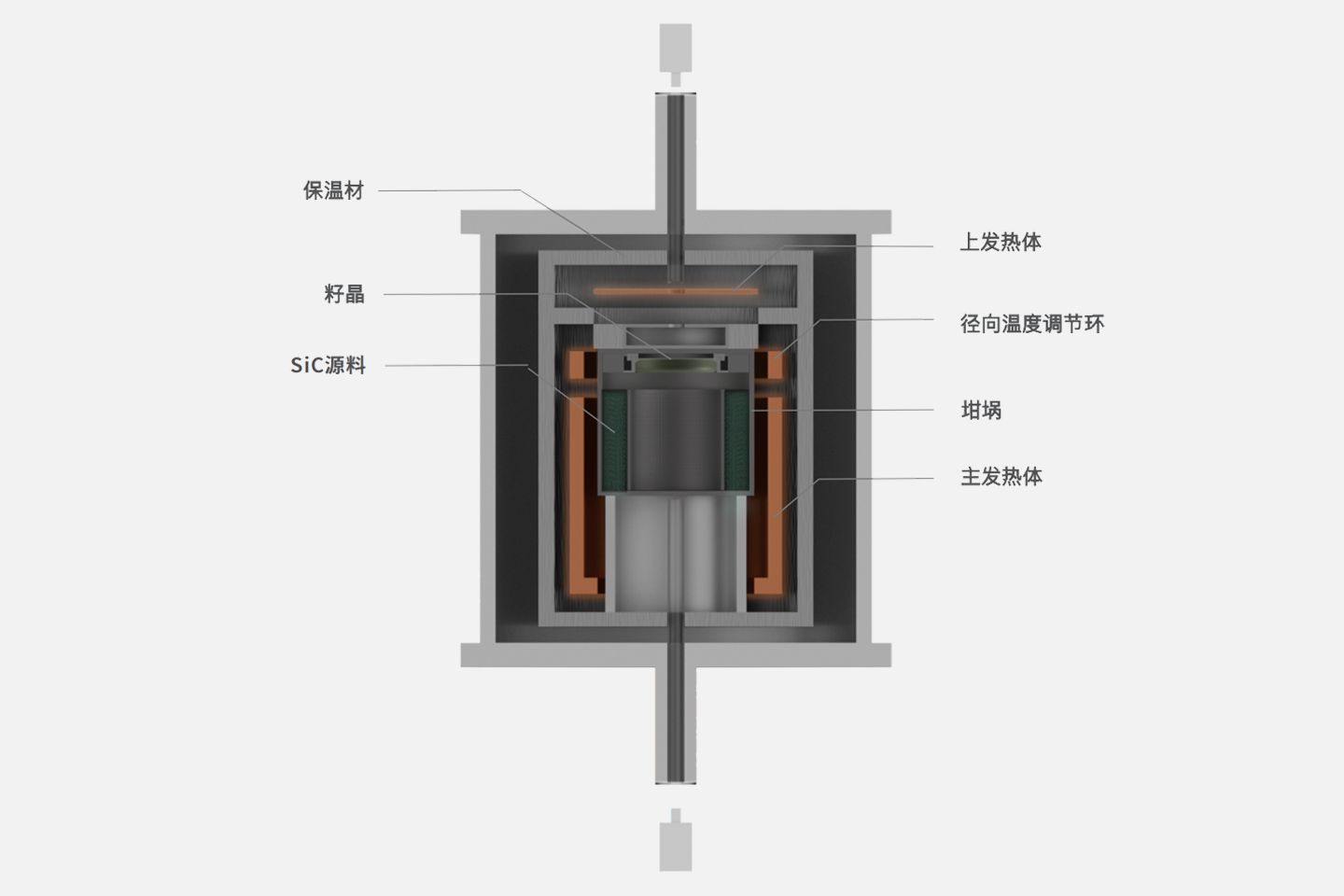
6、Silicon carbide crystal growth:
PVT Physical vapor transport method (mainstream)
HT-CVD High-temperature chemical vapor deposition method (high-quality semi-insulating)
LPE Liquid Phase Epitaxy (P-type silicon carbide)
7、Diamond crystal growth and graphene films: MPCVD Microwave Plasma Chemical Vapor Deposition
8、Gallium nitride crystal growth: HVPE Hydride Vapor Phase Epitaxy
9、Epitaxial growth processes: Heteroepitaxy and Homoepitaxy furnaces (e.g., sapphire-gallium nitride):
MOCVD Metal-organic Chemical Vapor DepositionA new type of vapor-phase epitaxial growth technology using metal organic compounds (high popularity, good quality)
VPE Vapor Phase Epitaxy (thick epitaxial layers, can change doping concentration and type, high impurity content, low precision)
MBE Molecular Beam Epitaxy (mainly used for gallium arsenide epitaxy, not suitable for large-scale production, high precision, expensive equipment, experimental use)
CBE Chemical Beam Epitaxy (not sustainable, experimental use)
IBE Ion Beam Epitaxy (not sustainable, experimental use)
Plasma etching equipment Etcher: Micro laser groove etching process
Physical vapor deposition equipment PVD: Physical deposition, magnetron sputtering, coating, etc.
Chemical vapor deposition equipment CVD: Includes MOCVD, PECVD, and other epitaxial equipment mentioned aboveOxide diffusion equipment Oxide/Diff: Silicon dioxide oxidation furnace
Atomic layer deposition equipment ALD: A new type of epitaxial process, under development.
Related product links
Silicon Carbide Wafer (SiC Wafer)
As semiconductor technology advances, Gallium Nitride (GaN) has become a core material in optoelectronics, rad...
With the rapid advancement of third-generation semiconductor technologies, Silicon Carbide (SiC) has emerged a...
As third-generation semiconductor materials such as silicon carbide (SiC) and gallium nitride (GaN) continue t...