Gallium nitride (GaN), as one of the core materials for third-generation wide-bandgap semiconductors, possesses excellent properties such as high breakdown field strength, high saturation electron drift velocity, strong radiation resistance, and good chemical stability. It is an ideal material for the production of wide-spectrum, high-power, high-efficiency optoelectronics, power electronics, and microelectronics.
There are many remarkable features of gallium nitride. Currently, the best application is the growth of high-quality gallium nitride epitaxial layers using gallium nitride as a substrate. The internal defect density of these epitaxial layers can be reduced to one thousandth of that grown on sapphire substrates, effectively lowering the junction temperature of LEDs and increasing the luminance by more than ten times per unit area.
Although gallium nitride is excellent, it is unfortunate that "GaN cannot be melted under atmospheric pressure and decomposes into Ga and N2 at high temperatures. The decomposition pressure at its melting point (2300°C) is as high as 6 GPa, which is difficult for current growth equipment to withstand. Therefore, traditional melt-growth methods cannot be used for the growth of GaN single crystals."
Compared to conventional semiconductor materials, the growth of GaN single crystals progresses slowly, and the crystal size is small, leading to high costs. Consequently, due to the limitations of GaN single crystal substrate size, production capacity, and cost, current GaN-based devices are primarily fabricated using epitaxial layers on heterogeneous substrates such as silicon, silicon carbide, and sapphire. The lack of GaN single crystal substrates has become a bottleneck for the development of GaN devices. Currently, the market price for this limited GaN material is quite high, and it is difficult to obtain.
Since most GaN devices are currently obtained through epitaxy on heterogeneous substrates, the functional epitaxial layers of the devices inevitably have stress and corresponding defects caused by lattice and thermal mismatches, thus affecting the performance and reliability of the devices. Homogeneous epitaxy on high-quality GaN single crystals effectively addresses these key issues, and the preparation technology of high-quality GaN single crystals has garnered significant attention from the academic and industrial communities.
In recent years, significant progress has been made domestically and internationally in the preparation of GaN single crystal substrates. Currently, the main methods for growing bulk GaN single crystal substrates include hydride vapor phase epitaxy (HVPE), ammonothermal method, and flux-assisted method (NaFlux), with HVPE being the most mainstream method.
Since the development of buffer layer technology by Japanese scientists in the 1980s, the growth of GaN by vapor phase epitaxy has experienced rapid advancement. HVPE growth technology, due to its advantages of atmospheric pressure growth, high growth rate, and feasibility for large-scale production, is currently the mainstream method for commercial production of GaN single crystal substrates.
The HVPE reactor mainly consists of two reaction zones. The first zone is the low-temperature region, typically at a temperature of 850°C, where the reaction between metallic Ga and HCl occurs, converting the liquid Ga metal into gaseous GaCl, which is then transported to the substrate region via a carrier gas. The second zone is the high-temperature region at 1040°C, where GaCl reacts with NH3 to achieve the growth of GaN single crystals on the substrate.
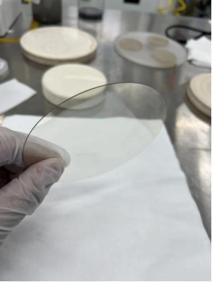
Currently, we have gallium nitride seed crystal products with diameters ranging from 105 to 110 mm and thicknesses of 450 to 600 µm. These gallium nitride seed crystals are undoped, as shown in the figure below. We welcome your attention and interest!

Related product links
Gallium Nitride Wafer (GaN Wafer)
As semiconductor technology advances, Gallium Nitride (GaN) has become a core material in optoelectronics, rad...
With the rapid advancement of third-generation semiconductor technologies, Silicon Carbide (SiC) has emerged a...
As third-generation semiconductor materials such as silicon carbide (SiC) and gallium nitride (GaN) continue t...