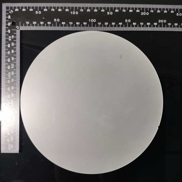
8-inch sapphire substrates play a crucial role in the manufacturing of modern electronic and optoelectronic devices. With their excellent thermal conductivity, mechanical strength, and chemical resistance, they are widely used in fields such as LEDs, lasers, and RF devices. This article will explore the specific applications and advantages of 8-inch sapphire substrates in Micro LEDs, HEMTs devices, and carrier wafers, highlighting their significant contributions to improving device performance and production efficiency.

Importance of High-Quality Sapphire CMP Surface
Achieving a high-quality sapphire CMP (chemical mechanical polishing) surface is vital for various applications. Our company utilizes high-precision inspection instruments and years of CMP process development to obtain higher-quality sapphire surfaces, addressing potential issues in various applications, and improving production yield and efficiency.
1. Blue-Green Micro LED
Sapphire substrates play a key role in Micro LED technology, mainly serving as the growth base for the LED light-emitting layer. The selection of sapphire substrates is based on the specific requirements of the equipment and LED devices. As one of the preferred materials for making LED chips, sapphire substrates are crucial in the manufacturing of Micro LEDs. Through semiconductor processes such as epitaxial growth, etching, deposition, and metal evaporation on the sapphire substrate, the Micro LED chip structure is eventually formed and shipped in wafer form.
High-Quality Surface: The abrasives used in CMP can cause tiny scratches on the sapphire substrate surface that are difficult to observe. Using our E1000 surface inspection equipment, these scratches can be clearly seen, matching the precision of the Candela 8720 inspection equipment. These micro-scratches on the sapphire substrate can affect epitaxial growth and make yield uncontrollable (as shown in Figure 1).

By continuously optimizing CMP abrasives and polishing processes through high-end inspection equipment, we can minimize these micro-scratches on the sapphire surface, ensuring substrate surface quality and improving subsequent process yields (as shown in Figure 2).

2. Sapphire-Based HEMTs Devices
High Electron Mobility Transistors (HEMTs) are key electronic devices widely used in high-frequency and high-power fields such as communications, radar, and satellite systems. The 8-inch sapphire substrate has significant application advantages in HEMTs devices:
Excellent Insulation: Sapphire has outstanding electrical insulation properties, which is particularly important for HEMTs devices operating in high-frequency environments. It effectively reduces leakage current, enhancing device stability and reliability.
High-Temperature Stability: Sapphire maintains stability in high-temperature processes and environments, which is crucial for the manufacturing and operation of HEMTs devices, ensuring their performance and lifespan.
Surface Quality Optimization: Using high-end inspection equipment like E1000 and Candela 8720, micro-scratches on the sapphire substrate surface can be clearly identified and eliminated. After optimizing the CMP process, the surface quality of the sapphire substrate is significantly improved, thus enhancing the quality of epitaxial growth and process yield.
3. Sapphire Carrier Wafer
In semiconductor manufacturing, sapphire substrates are widely used as carrier wafers, primarily providing support and protection. Specific applications of 8-inch sapphire substrates in carrier wafers include:
Support and Protection: When handling thin and brittle semiconductor materials, sapphire carrier wafers provide necessary support and protection, preventing the substrate from cracking or damage during processing.
Thermal Stability: The thermal stability of sapphire material ensures it maintains shape and size stability in high-temperature processes, preventing thermal deformation from affecting semiconductor devices.
Conclusion
The application of 8-inch sapphire substrates in Micro LEDs, HEMTs devices, and carrier wafers fully demonstrates their mechanical strength, high-quality surface, and thermal stability. Through our company's high-precision inspection and optimized CMP processes, sapphire substrates can provide a more reliable support platform for semiconductor and electronic device manufacturing, ensuring efficient and high-quality epitaxial growth and subsequent processes. In these high-tech fields, sapphire substrates are indispensable, providing a solid foundation for the development of modern electronic technology.
Related product links
Sapphire Substrate Wafer