In the semiconductor manufacturing field, epitaxial growth processes are crucial technologies, among which silicon epitaxy and silicon carbide epitaxy are two important types. They differ significantly in terms of materials, applications, processes, and characteristics, as detailed below.
Materials and Applications
Silicon Epitaxy:
Silicon epitaxy involves the growth of a high-quality single-crystal silicon film on a silicon substrate using chemical vapor deposition (CVD) techniques. Silicon (Si), as the primary material, is widely used in traditional semiconductor devices, including metal-oxide-semiconductor field-effect transistors (MOSFETs), complementary metal-oxide-semiconductor (CMOS) devices, and various integrated circuits. Silicon epitaxy technology forms the foundation of the modern silicon-based semiconductor industry, supporting the widespread adoption and development of large-scale integrated circuits.
Silicon Carbide Epitaxy:
Silicon carbide epitaxy entails the growth of high-quality silicon carbide (SiC) films on SiC substrates, also achieved through CVD techniques. Silicon carbide boasts superior properties such as wide bandgap, high thermal conductivity, high breakdown electric field, and high electron saturation velocity, making it highly suitable for high-temperature, high-frequency, and high-power electronic devices. These include power electronics (e.g., MOSFETs, IGBTs), radio-frequency devices, and high-temperature sensors. SiC epitaxial layers excel in applications requiring high efficiency and high power density, such as electric vehicles, power grids, and industrial drives.
Process Differences
Silicon Epitaxy:
Growth Temperature: Typically ranges from 900°C to 1250°C.
Source Materials: Primarily uses silane (SiH4) or chlorosilanes (e.g., SiCl4).
Growth Method: Utilizes chemical vapor deposition (CVD) technology.
Thickness Control: Can grow epitaxial layers from tens of nanometers to several micrometers thick.
Silicon Carbide Epitaxy:
Growth Temperature: Generally ranges from 1300°C to 1600°C.
Source Materials: Mainly uses silane (SiH4) and carbon-containing gases (e.g., propane, C3H8).
Growth Method: Also employs CVD technology but requires higher temperatures and more precise control.
Thickness Control: Typically grows epitaxial layers from several micrometers to tens of micrometers thick.
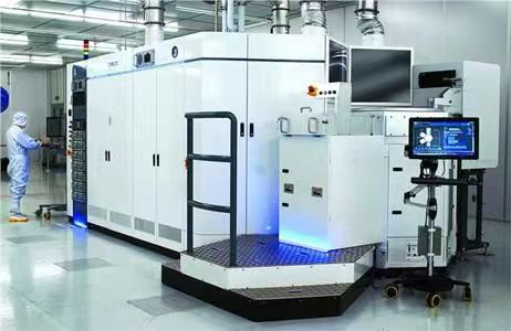
Following are our Epitaxial equipments:

Characteristics and Challenges
Silicon Epitaxy:
Advantages: Mature process, lower cost, suitable for the mass production of integrated circuits.
Challenges: Performance is limited in high-temperature, high-frequency, and high-power applications.
Silicon Carbide Epitaxy:
Advantages: Features wide bandgap, high thermal conductivity, high breakdown electric field, and high electron saturation velocity, making it highly advantageous for high-temperature, high-frequency, and high-power applications.
Challenges: Complex preparation process, higher cost, stringent material quality control requirements, particularly in avoiding dislocations and defects.
Conclusion
Silicon epitaxy and silicon carbide epitaxy each have distinct characteristics in terms of materials, applications, processes, and properties. Silicon epitaxy technology dominates the manufacturing of traditional semiconductor devices, with its mature processes and lower costs supporting a wide range of electronic products and integrated circuits. However, as the demand for high-performance, high-power electronic devices grows, silicon carbide epitaxy technology, with its superior physical properties, demonstrates great potential in high-temperature, high-frequency, and high-power applications. Although the preparation and quality control of silicon carbide epitaxy are relatively complex and costly, its irreplaceable value in specific applications drives continuous technological advancements and expanded usage.
Related product links
As semiconductor technology advances, Gallium Nitride (GaN) has become a core material in optoelectronics, rad...
With the rapid advancement of third-generation semiconductor technologies, Silicon Carbide (SiC) has emerged a...
As third-generation semiconductor materials such as silicon carbide (SiC) and gallium nitride (GaN) continue t...
