In solid-state physics, the term "bandgap" refers to the energy difference between the valence band and the conduction band in solid materials. The valence band is the energy level region filled with electrons, while the conduction band is the region where electrons can move freely. The presence of a bandgap determines the electrical properties of the material.
Silicon carbide (SiC) and gallium nitride (GaN) are two wide bandgap semiconductor materials, characterized as follows:
Silicon carbide (SiC) typically has a bandgap ranging from 2.2 to 3.3 electron volts (eV), depending on its crystal structure and doping level. Single-crystal SiC generally has a higher bandgap value, typically between 2.3 and 3.3 eV. In comparison, gallium nitride (GaN) typically has a bandgap ranging from 3.4 to 3.6 eV, slightly exceeding that of silicon carbide in some aspects.
Wide bandgap semiconductor materials offer several advantages:
Firstly, they possess high thermal stability and resistance to high temperatures, maintaining good electrical performance in high-temperature environments without easily failing. Secondly, they exhibit high electron drift velocity and low parasitic capacitance, enabling operation at high frequencies and withstand high voltage operations. Additionally, wide bandgap materials typically have low leakage currents, contributing to reduced power losses. Lastly, they can withstand higher power densities, suitable for high-power electronic devices and optoelectronic devices.
As wide bandgap semiconductor materials, silicon carbide and gallium nitride find widespread applications in various fields:
Silicon carbide plays a significant role in the field of power electronic devices, such as inverters and solar inverters, which require high voltage, high temperature, and high-frequency power converters. Additionally, silicon carbide is widely used in optoelectronic devices, such as blue LEDs and laser diodes.
Gallium nitride excels in high-power density devices, suitable for power amplifiers, RF power amplifiers, and microwave devices in applications like 5G communication base stations and radar systems. Furthermore, gallium nitride finds broad applications in optoelectronic devices, such as blue LEDs and lasers.
Although silicon carbide and gallium nitride already possess wide bandgaps, there is still potential to further widen their bandgaps theoretically. Methods such as alloying, strain engineering, nanoscale structuring, and doping may further increase the bandgap of silicon carbide and gallium nitride. However, achieving a significantly wider bandgap may require overcoming challenges such as material stability, control of growth processes, and uniform distribution of impurities. Thus, while theoretically possible, achieving a significantly wider bandgap may necessitate further research and technological breakthroughs.
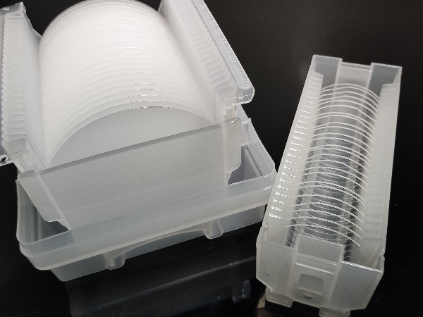
Furthermore, the fabrication of Silicon Carbide Wafers and gallium nitride wafers has been a key focus in the semiconductor industry. These wafers serve as the substrate for the growth of silicon carbide and gallium nitride epitaxial layers, enabling the production of high-performance electronic and optoelectronic devices.
| Materials | Bandgap(eV) | ||
| Si | 1.1 | ||
| SiC | 2.2-3.3 | ||
| GaN | 3.4-3.6 | ||
| AIGaN | 2.9-6.2 | ||
| AIN | 6.0 |
As semiconductor technology advances, Gallium Nitride (GaN) has become a core material in optoelectronics, rad...
With the rapid advancement of third-generation semiconductor technologies, Silicon Carbide (SiC) has emerged a...
As third-generation semiconductor materials such as silicon carbide (SiC) and gallium nitride (GaN) continue t...