At the forefront of semiconductor technology, silicon carbide homogeneous epitaxy offers a multitude of advantages, enabling groundbreaking innovations across various industries. So JXT Technology Co.,Ltd. is excited to explore the material characteristics, advantages, applications, and research value of 4H-N SiC epitaxial films in this blog.
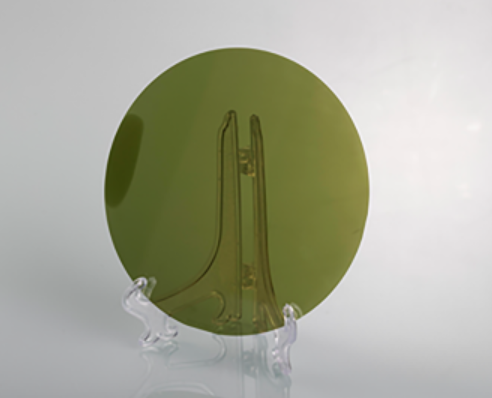
The typical specification of SiC on SiC Homogeneous Epitaxy

Advantages of 4H-N SiC Homogeneous Epitaxy
1.High Electrical Conductivity:
Silicon Carbide homogeneous epitaxial wafers offer excellent electrical conductivity, making them ideal for power semiconductor devices like Schottky diodes and MOSFETs. The high electron mobility allows for reduced switching losses and improved device efficiency.
2.Excellent Thermal Stability:
Silicon Carbide homogeneous epitaxial wafers maintain their electrical properties even under extreme temperature conditions. This quality ensures long-term stability and reliability in high-temperature applications, such as in aerospace and automotive industries.
3.Compatibility with Silicon Carbide Substrates:
Growing N-type SiC epi-layer on 4H-N silicon carbide substrates allows for seamless integration with existing SiC-based technology, ensuring a smooth transition for manufacturers and researchers.
Applications
1.Power Electronics:
Silicon Carbide homogeneous epitaxial wafers are revolutionizing the power electronics industry. They are used in high-voltage Schottky diodes and MOSFETs, enabling efficient energy conversion and reduced power losses in electric vehicles, renewable energy systems, and more.
2.High-Temperature Sensors:
The exceptional thermal stability of Silicon Carbide homogeneous epitaxial wafers makes it suitable for high-temperature sensor applications in aerospace, gas turbine engines, and industrial processes. These sensors can operate reliably in extreme environments.
3.Optoelectronic Devices:
Silicon Carbide homogeneous epitaxial wafers is being explored for optoelectronic applications, including ultraviolet photodetectors and light-emitting diodes (LEDs). Its wide bandgap and high thermal conductivity offer unique advantages in these fields.
The study of silicon carbide homogeneous epitaxy holds immense research value. Researchers are continually exploring new techniques to enhance the growth of epitaxial films and optimize material properties. As a third-generation semiconductor material, Silicon Carbide homogeneous epitaxial wafers contributes to advancements in power electronics, high-temperature sensors, and optoelectronics, driving innovation in multiple industries.
In conclusion, silicon carbide homogeneous epitaxy is a material of significant promise and potential. Its exceptional material characteristics, numerous advantages, diverse applications, and ongoing research efforts solidify its position as a critical player in the semiconductor materials industry. With its unique properties and adaptability, Silicon Carbide homogeneous epitaxial wafers are opening new horizons in the world of technology.
As semiconductor technology advances, Gallium Nitride (GaN) has become a core material in optoelectronics, rad...
With the rapid advancement of third-generation semiconductor technologies, Silicon Carbide (SiC) has emerged a...
As third-generation semiconductor materials such as silicon carbide (SiC) and gallium nitride (GaN) continue t...