In the semiconductor industry, particularly in the field of third-generation semiconductors (wide-bandgap semiconductors), the roles of the substrate and epitaxial layer are crucial. The substrate serves as the foundation for semiconductor devices, while the epitaxial layer enhances device performance through advanced growth techniques. So, what exactly distinguishes the substrate from the epitaxial layer, and how do they each contribute to semiconductor device manufacturing?

1. What is a Substrate?
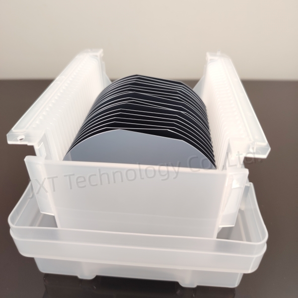
The substrate is the foundational material in semiconductor manufacturing. Typically composed of single-crystal semiconductor materials such as silicon (Si), gallium arsenide (GaAs), or silicon carbide (SiC), it undergoes a series of precise processes, including cutting, grinding, and polishing, to form a wafer. The primary function of the substrate is to provide a stable and lattice-matched platform for the subsequent growth of other materials. During the manufacturing process, the substrate can either be used directly for device fabrication or serve as a base for epitaxial growth to enhance device performance.
For example, in silicon carbide (SiC) devices, the SiC substrate not only acts as a mechanical support but also plays a key role in determining the final electrical characteristics of the device. As such, the quality and properties of the substrate are critical to device performance, particularly in the third-generation semiconductor materials, where wide-bandgap materials such as SiC and GaN have become essential.
2. What is Epitaxy?
Epitaxy refers to the process of growing a single-crystal thin layer, known as the epitaxial layer, on top of the substrate. This layer can be composed of the same material as the substrate (homoepitaxy) or a different material (heteroepitaxy). The epitaxial layer, typically only a few micrometers thick, aligns with the crystal structure of the substrate and is grown using techniques such as Chemical Vapor Deposition (CVD) or Molecular Beam Epitaxy (MBE), which allow for precise control over its crystal structure, resistivity, and thickness.
In traditional silicon semiconductor devices, epitaxy is widely used. For example, by growing a high-resistivity epitaxial layer on a low-resistivity silicon substrate, devices can achieve both high breakdown voltage and low saturation voltage, greatly improving power device efficiency. In third-generation semiconductors, the epitaxial layer largely determines the final device performance, with parameters such as the thickness and carrier concentration of the epitaxial layer directly influencing the electrical characteristics of SiC devices.
3. Key Differences Between Substrate and Epitaxy
Functional Difference
Substrate serves as the foundational crystal structure, providing mechanical stability and initial crystallographic properties for subsequent layers.
Epitaxial layer is the thin crystalline layer grown on the substrate, which primarily defines the critical electronic properties of the semiconductor device, such as conductivity, breakdown voltage, and carrier concentration.
Material and Process
The substrate is typically made from materials like silicon, gallium arsenide, or silicon carbide. It provides a stable platform that is lattice-matched with the epitaxial layer.
The epitaxial layer can be grown from the same material as the substrate (e.g., silicon on silicon) or from a different material (e.g., gallium nitride on sapphire). By controlling the thickness, crystallographic orientation, and growth conditions, the epitaxial layer enables complex device functionalities.
Functional Mechanism
The substrate primarily supports the device mechanically and electrically, while the epitaxial layer defines the functional properties of the final device. For example, in SiC devices, the substrate provides mechanical support, but the epitaxial layer, through precise control of its thickness and carrier concentration, determines the high-voltage performance of the device.
4. Applications of Substrate and Epitaxy in Third-Generation Semiconductors
Third-generation semiconductors, such as SiC and GaN, are widely used in high-power and high-frequency devices. In particular, for SiC devices, the quality and properties of the epitaxial layer are crucial. While the SiC substrate serves as a mechanical foundation, the device’s electrical performance—such as high breakdown voltage and low saturation voltage—is primarily determined by the epitaxial layer’s thickness and background carrier concentration.
For high-voltage applications, SiC epitaxial materials must meet stringent requirements regarding thickness and carrier concentration, making epitaxy a critical technology for optimizing the performance of SiC devices. In fact, nearly all SiC power devices are fabricated on high-quality SiC epitaxial wafers, underscoring the vital role that epitaxial growth plays in the wide-bandgap semiconductor industry.
Conclusion
Substrate and epitaxy are indispensable components of semiconductor manufacturing, each playing a distinct role. The substrate serves as the foundational material, providing the crystal structure and mechanical support, while the epitaxial layer is responsible for optimizing the semiconductor device’s performance, particularly in high-power, high-frequency, and high-voltage applications. As third-generation semiconductor materials rapidly evolve, epitaxy has become a critical technology for enhancing device performance, especially in wide-bandgap semiconductors, where the quality of the epitaxial layer directly impacts device efficiency and reliability.
As semiconductor technology advances, Gallium Nitride (GaN) has become a core material in optoelectronics, rad...
With the rapid advancement of third-generation semiconductor technologies, Silicon Carbide (SiC) has emerged a...
As third-generation semiconductor materials such as silicon carbide (SiC) and gallium nitride (GaN) continue t...