Third-generation semiconductor materials possess material performance advantages that are unparalleled by silicon materials. When considering characteristics such as the bandgap width, thermal conductivity, and breakdown field, third-generation semiconductors outperform silicon. Consequently, the introduction of third-generation semiconductors can effectively address the limitations of silicon materials, improving device heat dissipation, conduction losses, high-temperature operation, high-frequency capabilities, and more. It is hailed as a new engine for industries like optoelectronics and microelectronics.
Among them, Gallium Nitride (GaN) boasts extensive versatility and is considered one of the most important semiconductor materials following silicon. Compared to the widely used silicon-based power devices, GaN power devices exhibit higher critical electric field strength, lower on-state resistance, faster switching frequencies, enabling higher system efficiency and operation at elevated temperatures.
Presently, GaN-based devices are primarily fabricated on heterogeneous substrates such as silicon and sapphire. This has resulted in the lagging development of GaN single-crystal substrates and homoepitaxial devices compared to applications based on heteroepitaxial devices.
Sapphire (α-Al2O3), also known as corundum, is the most widely used LED substrate material in commercial applications, dominating a significant share of the LED substrate market. In its early applications, sapphire substrates demonstrated their unique advantages. The GaN thin films grown on sapphire substrates exhibit a dislocation density comparable to those grown on SiC substrates. Additionally, sapphire utilizes the melt-growth technique, which is a more mature process. This allows for the production of larger-sized, high-quality single crystals at a lower cost, making it suitable for industrial development. Consequently, sapphire is the earliest and most extensively used substrate material in the LED industry.
2. Single Crystal Silicon
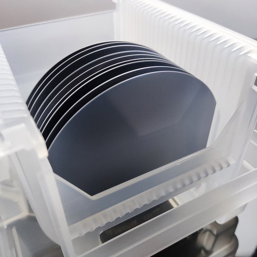
Silicon is currently the most widely used and technologically mature semiconductor material. Due to the high maturity of single crystal silicon growth technology, it is easy to obtain low-cost, large-sized (6-12 inches), high-quality substrates, significantly reducing the cost of LED production. Furthermore, since single crystal silicon has already been extensively used in the field of microelectronics, using single crystal silicon substrates enables the direct integration of LED chips with integrated circuits, promoting the miniaturization of LED devices. In addition, single crystal silicon offers some advantages over the most widely used LED substrate, sapphire. It has higher thermal conductivity, good electrical conductivity, and the ability to fabricate vertical structures, making it more suitable for high-power LED production.
As semiconductor technology advances, Gallium Nitride (GaN) has become a core material in optoelectronics, rad...
With the rapid advancement of third-generation semiconductor technologies, Silicon Carbide (SiC) has emerged a...
As third-generation semiconductor materials such as silicon carbide (SiC) and gallium nitride (GaN) continue t...