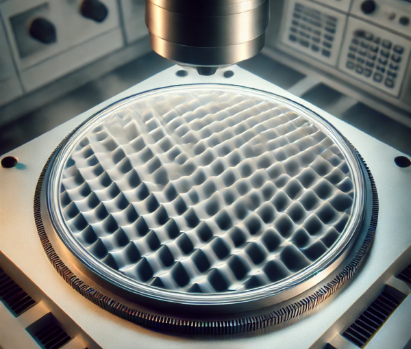
As a third-generation semiconductor material, silicon carbide (SiC) boasts high breakdown electric field strength, a wide bandgap, and high thermal conductivity, making it widely applicable in power electronics, RF devices, and high-temperature sensing. In SiC device manufacturing, the thickness of the epitaxial layer is a crucial parameter affecting performance. Does a thicker SiC epitaxial layer always yield better results? How should the epitaxial layer thickness be optimized for different applications? This article provides a technical analysis of the impact of SiC epitaxial layer thickness and introduces JXT's customized epitaxial wafer solutions.
1. Functions and Control of SiC Epitaxial Layer Thickness
1.1 Key Functions of the SiC Epitaxial Layer
The SiC epitaxial layer, grown on an SiC substrate using chemical vapor deposition (CVD), serves several critical functions:
Provides high breakdown voltage: Enhances voltage withstand capability in high-power devices.
Regulates carrier transport properties: Optimizes doping concentration to reduce on-resistance (R).
Reduces parasitic capacitance: Improves performance in RF and high-frequency microwave devices.
Enhances device stability: Improves resistance to high temperatures and radiation, making it suitable for extreme environments.
1.2 Key Parameters Affecting SiC Epitaxial Layer Thickness
The thickness of the SiC epitaxial layer is influenced by device application, doping concentration, and growth process. Typical parameters include:
Epitaxial layer thickness range: 0.1 μm to 40 μm
Doping concentration: 10¹³ cm⁻³ to 10¹⁹ cm⁻³ (controlled using N, P, and Al dopants)
Crystal orientation: Primarily 4H-SiC (high electron mobility), with some applications of 6H-SiC
Growth rate: Typically 5-10 μm/h using CVD equipment; high-speed growth up to 20-30 μm/h may lead to increased defect density
2. Relationship Between SiC Epitaxial Thickness and Applications
2.1 Power Electronics: Epitaxial Thickness and Voltage Withstanding Capability
In SiC MOSFETs, Schottky barrier diodes (SBDs), IGBTs, and other power electronic devices, the thickness of the epitaxial layer directly determines the voltage withstand capability. Generally, a thicker epitaxial layer supports higher voltage ratings, but it also increases on-resistance, impacting device efficiency.
Epitaxial Thickness vs. Voltage Withstanding Capability
| Voltage Rating | Epitaxial Thickness | Typical Doping Concentration |
| 600V | 5-10 μm | 1×10¹⁶ cm⁻³ |
| 1200V | 10-15 μm | 8×10¹⁵ cm⁻³ |
| 1700V | 15-20 μm | 5×10¹⁵ cm⁻³ |
| 3300V | 30-40 μm | 1-3×10¹⁵ cm⁻³ |
2.2 RF and Microwave Devices: Epitaxial Layers Should Be as Thin as Possible
SiC is widely used as a substrate for GaN-on-SiC high-electron-mobility transistors (HEMTs) in 5G base stations, radar, and satellite communications, offering exceptional high-frequency performance.
Epitaxial Thickness vs. High-Frequency Performance
| Application Field | Typical Epitaxial Thickness | Optimization Objective |
| 5G GaN-on-SiC | 0.1-0.5 μm | Reduce parasitic capacitance, improve high-frequency response |
| Millimeter-Wave Radar | 0.3-1 μm | Increase power gain, optimize frequency response |
| High-Frequency Power Amplifiers | <1 μm | Improve device speed |
3. JXT SiC Epitaxial Wafer Recommendations
JXT provides high-quality SiC epitaxial wafers ranging from 2 inches to 8 inches in diameter, with customizable epitaxial thickness, doping concentration, and crystal orientation based on customer requirements.
3.1 Advantages of JXT SiC Epitaxial Wafers
Wide range of sizes: Available from 2-inch to 8-inch SiC epitaxial wafers, catering to power electronics and RF applications.
Custom solutions: Customers can specify epitaxial thickness (0.1 μm - 40 μm) and doping concentration to meet their unique application needs.
High-quality epitaxial growth: Advanced CVD technology ensures low defect density and high uniformity.
Fast delivery: Efficient production processes enable short lead times and support for large-volume orders.
3.2 Application Areas
JXT SiC epitaxial wafers are widely used in:
Electric Vehicles (EVs): SiC MOSFET inverters.
Photovoltaics & Industrial Power Supplies: High-voltage power devices.
5G & Telecommunications: GaN-on-SiC HEMTs.
Aerospace & Specialty Electronics: High-temperature sensors, satellite communications.
JXT offers tailored SiC epitaxial wafer solutions to meet diverse market demands. Contact us for more product information!
As semiconductor technology advances, Gallium Nitride (GaN) has become a core material in optoelectronics, rad...
With the rapid advancement of third-generation semiconductor technologies, Silicon Carbide (SiC) has emerged a...
As third-generation semiconductor materials such as silicon carbide (SiC) and gallium nitride (GaN) continue t...