With the continuous advancement of display technology, Micro-LED has gained significant market attention as the next-generation display solution due to its high brightness, high contrast, low power consumption, and long lifespan. Among various substrate materials, GaN-on-Silicon epitaxial wafers stand out as a key choice for industrialization due to their large-scale production capability, cost-effectiveness, and compatibility with CMOS technology. This article provides a detailed overview of the structure, advantages, key parameters, and application prospects of GaN-on-Silicon epitaxial wafers.
1. Structure of GaN-on-Silicon Epitaxial Wafers
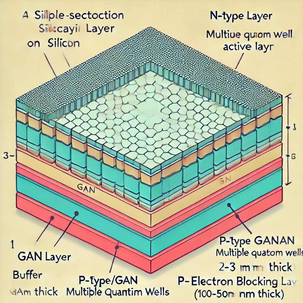
GaN-on-Silicon epitaxial wafers primarily consist of the following layers:
GaN-on-Silicon Substrate: High-resistivity or low-resistivity silicon substrate with (111) orientation, serving as the foundation for GaN epitaxial growth.
Buffer Layer: An AlN or AlN/GaN composite buffer layer to mitigate the lattice mismatch (~17%) and thermal expansion coefficient mismatch between GaN and Si, reducing defect density and preventing cracks.
GaN Epitaxial Layer:
n-type GaN Layer (1–3 μm thick): Provides the electron transport channel.
InGaN/GaN Multiple Quantum Well (MQW) Active Layer (2–3 nm thick quantum wells): Responsible for light emission with adjustable wavelengths.
p-type GaN Layer (100–500 nm thick): Forms the p-n junction to enable carrier recombination.
p-type AlGaN Electron Blocking Layer (EBL) (10–50 nm thick): Prevents electron leakage and enhances luminous efficiency.
2. Key Advantages
1) Large-Scale Production and Cost Reduction
Compared to sapphire and silicon carbide (SiC) substrates, silicon substrates can be scaled up to 8-inch or even 12-inch sizes, improving Micro-LED chip production efficiency and reducing manufacturing costs.
2) CMOS Compatibility for Easy Integration
Silicon is the mainstream material in the semiconductor industry. GaN-on-Silicon Micro-LEDs can seamlessly integrate with CMOS driver circuits, enabling compact and efficient display modules.
3) High Brightness and Long Lifespan
GaN-based Micro-LEDs offer superior optoelectronic performance, including high luminous efficiency and stability. Compared to OLED and LCD technologies, Micro-LEDs have a significantly longer lifespan.
4) Low Power Consumption for Portable and Miniature Displays
Micro-LEDs consume significantly less power than traditional LCD and OLED displays, making them ideal for wearable devices, AR/VR headsets, and other portable electronics.
3. Key Parameters
| Parameter | Typical Value |
| GaN-on-Silicon Substrate | (111) orientation, 2"–8" size, thickness 525±25 μm |
| Buffer Layer | AlN or AlN/GaN, thickness 100–500 nm |
| n-type GaN Layer | 1–3 μm, doping concentration ~ cm⁻³ |
| MQW Active Layer | 3–10 quantum wells, tunable wavelength 450–550 nm |
| p-type GaN Layer | 100–500 nm, doping concentration ~ cm⁻³ |
| Emission Wavelength | 450 nm (blue), 520 nm (green) |
| Operating Voltage | 3.2–3.5V (Micro-LED) |
4. Application Prospects
1) Micro-LED Displays
GaN-on-Silicon epitaxial wafers are suitable for AR/VR displays, smartwatches, micro-projectors, high-end TVs, and other display applications.
2) Visible Light Communication (LiFi)
Micro-LED-based visible light communication (VLC) technology enables high-speed data transmission, representing a key development in future wireless communication.
3) Miniature Projection
Micro-LED light sources, with their high brightness and low power consumption, are ideal for ultra-compact projectors and head-up display (HUD) systems.
5. We Provide High-Quality GaN-on-Silicon Epitaxial Wafers
We are committed to supplying high-quality GaN-on-Silicon epitaxial wafers with low defect density, high luminous efficiency, and excellent uniformity. Our products can be customized in various sizes (2"–8"), wavelengths (450 nm–550 nm), and doping concentrations to meet the demands of high-end display, LiFi communication, and miniature projection applications, with the capability for large-scale production.
If you have any technical inquiries or requirements for GaN-on-Silicon epitaxial wafers, feel free to contact us. Let's work together to drive the industrialization of Micro-LED display technology!
As semiconductor technology advances, Gallium Nitride (GaN) has become a core material in optoelectronics, rad...
With the rapid advancement of third-generation semiconductor technologies, Silicon Carbide (SiC) has emerged a...
As third-generation semiconductor materials such as silicon carbide (SiC) and gallium nitride (GaN) continue t...