What is CMP?
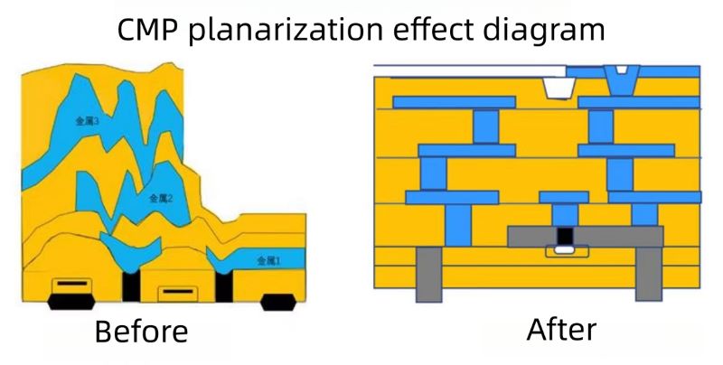
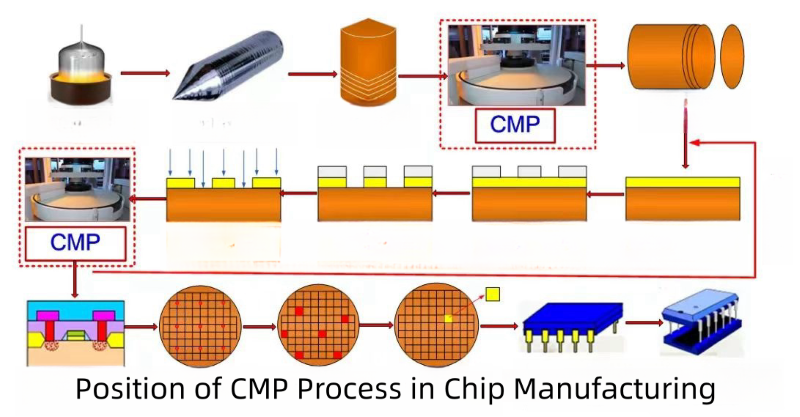
Chemical Mechanical Planarization (CMP) is a critical process in semiconductor manufacturing used to planarize the surface of semiconductor wafers. CMP combines both chemical and mechanical forces to remove material from the wafer surface, achieving a highly flat and smooth finish. The process involves the use of a slurry containing chemical agents that react with the wafer material and abrasive particles that mechanically polish the surface. A polishing pad applies pressure and movement to facilitate this dual action, ensuring uniform material removal across the wafer.

The Role of CMP in Silicon Carbide Wafer Manufacturing
In the context of silicon carbide (SiC wafer) wafer manufacturing, CMP plays a vital role due to the unique properties of SiC. Silicon carbide is known for its exceptional hardness and chemical inertness, making it an ideal material for high-power, high-temperature, and high-frequency applications. However, these properties also pose significant challenges in processing and surface planarization.
1. Surface Planarization
After the initial growth and cutting processes, SiC wafers often exhibit surface irregularities and defects. CMP is employed to achieve a highly planar surface, which is essential for subsequent photolithography and other microfabrication steps. A smooth and flat surface ensures the precision and accuracy required for the intricate patterns in semiconductor devices.
2. Removal of Damaged Layers
Mechanical processes used in wafer slicing and grinding can introduce defects and damaged layers on the SiC wafer surface. CMP effectively removes these damaged layers, resulting in a defect-free and uniformly smooth surface. This step is crucial for improving the reliability and performance of the final semiconductor devices.
3. Interface Quality Improvement
For SiC-based devices, particularly metal-oxide-semiconductor field-effect transistors (MOSFETs), the quality of the interface between the SiC wafer and the oxide layer is critical. A planarized surface provided by CMP ensures a high-quality interface, which enhances the electrical properties and overall performance of the device. A smooth interface reduces the likelihood of defects that can degrade the device's functionality.
4. Multilayer Structure Planarization
Advanced semiconductor devices often involve complex multilayer structures. CMP is used at various stages to planarize each layer, ensuring that subsequent layers can be deposited and patterned accurately. This is essential for the fabrication of high-performance and high-density integrated circuits.

Challenges in CMP for Silicon Carbide
The CMP process for SiC wafers presents several challenges due to the material's hardness and chemical stability:
Slurry and Pad Selection: The slurry must contain appropriate chemical agents that can effectively react with SiC, and the abrasive particles must be capable of mechanically polishing the hard surface. The polishing pad must also be durable enough to withstand the hardness of SiC while providing uniform pressure distribution.
Process Control: Precise control of CMP parameters such as pressure, speed, and slurry composition is necessary to achieve uniform material removal rates and high surface quality. Variations in these parameters can lead to non-uniform planarization and surface defects.
Defect Management: Minimizing surface defects such as scratches and pits is critical. Optimizing the CMP process to reduce such defects improves the overall quality and performance of the SiC wafers and the resulting devices.
Conclusion
CMP is an indispensable process in the manufacturing of silicon carbide wafers, addressing the challenges posed by SiC's hardness and chemical inertness. By achieving a highly planar and defect-free surface, CMP ensures the precision and reliability needed for advanced semiconductor devices. The continuous optimization of CMP parameters and materials is essential to meet the stringent requirements of modern semiconductor manufacturing and to fully exploit the benefits of silicon carbide in high-performance applications.
As semiconductor technology advances, Gallium Nitride (GaN) has become a core material in optoelectronics, rad...
With the rapid advancement of third-generation semiconductor technologies, Silicon Carbide (SiC) has emerged a...
As third-generation semiconductor materials such as silicon carbide (SiC) and gallium nitride (GaN) continue t...
