SiC on SiC:
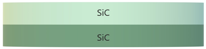
● Typical Structure: ● Typical Specification:
1.n-type SiC(N-doping)on SiC SiC layer thickness up to 100um on SiC
2.P-type SiC(Al-doping)on SiC SiC layer thickness up to 100um on SiC
3.SiC(undoped)on SiC SiC layer thickness up to 100um on SiC
4.Schottky diode Schottky diode structure
5.MOSFET MOSFET structure
6.PIN diode PIN diode structure
7.IGBT IGBT structure
8.JFET JFET structure
● Reference:
1"/2"/3"/ 4"/6" SiC substrate(10*10mm etc.) is available.
Up to 100µm SiC epitaxial layer on SiC
4H and 6H SiC substrates are available
CC range 1E15~1E19/cm³
RMS(AFM)<0.5nm
Thickness uniformity < 5%
Metal Contamination <1E11 atoms/cm2(K/Ca/Ti/V/Cr/Mn/Fe/Ni/Cu/Zn)
Off-Axis:0°~8°toward <11-20> SiC substrates are available.
N-type/semi-insulating SiC Substrates is available.
● Epitaxial structure and substrate specifications can be customized, anna@jxtwafer.com
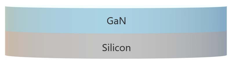
● Epitaxy structure:
● Advantages: low cost, good stability in high temperature, excellent mechanical properties, mature technology in LED field.
● Disadvantages: low thermal conductivity, the lattice mismatch in power devices, a little worse performance.
● Application:used in LED and optoelectronic fields.
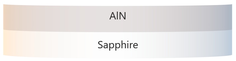
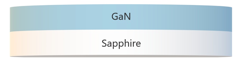
● Epitaxy structure:
● Advantages: low price of the substrates, good electrical and thermal conductivity, large-scale industrialization.
● Disadvantages: the lattice parameters of sillicon aren't matched to GaN very well , resulting in slightly poor wafer performance and low yield.
● Application: used in HEMT and chips for consumer electronics , RF chips,etc.
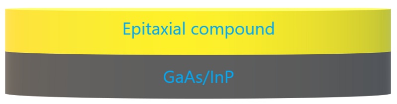
● Epitaxy structure:
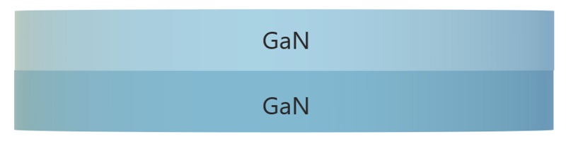
● Advantages: high temperature resistance, low loss, excellent performance.
● Disadvantages: limited supply of gallium nitride substrates, complicated technology, high cost, and low-scale industrialization.
● Application: used in blue light, green laser and other optoelectronic fields.
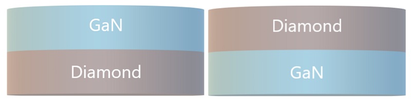
● Epitaxy structure:
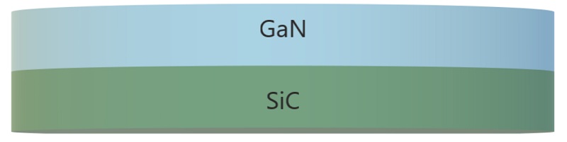
● Advantages: high thermal conductivity, good antistatic ability, excellent performance.
● Disadvantages: poor machining performance, high cost, limited application scenarios.
● Application: used in 5G base station RF chips, satellite radar, LED and optoelectronic fields.
If you want to know more epitaxial structures, please email us anna@jxtwafer.com.