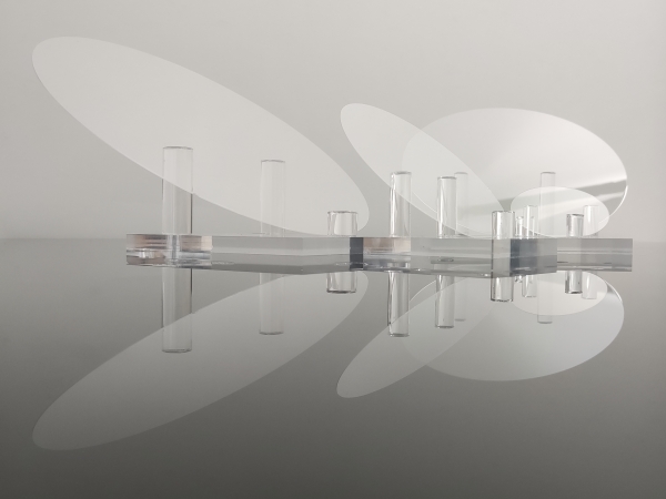
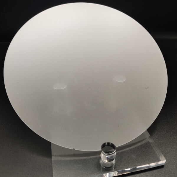
With the rapid advancement of high-tech industries, sapphire wafers, particularly in the 8-inch size, have become a critical material in the semiconductor and optoelectronic fields. Known for their exceptional mechanical strength, thermal stability, and optical properties, sapphire wafers are widely used in LED chip manufacturing, optical windows, and other high-tech devices. However, the production of 8-inch sapphire wafers presents significant challenges, including yield rates, cost control, and technical difficulties.
Yield Analysis
Compared to traditional 2-inch and 4-inch sapphire wafers, manufacturing 8-inch sapphire wafers is substantially more challenging. The key challenges include:
1. Crystal Growth Complexity: Larger sizes require more stable crystal growth techniques to avoid internal defects and stress concentrations.
2. Processing Complexity: Slicing, grinding, and polishing processes become exponentially more difficult as wafer size increases, directly impacting production yields.
3. Defect Control: Larger wafers demand higher crystal uniformity, as any inconsistencies can lead to localized performance issues in downstream processes.
Currently, the industry average yield ranges from 60% to 80%, while leading companies can achieve yields exceeding 90% through advanced process control and equipment.
Cost Analysis
The cost of 8-inch sapphire wafers is primarily influenced by the following factors:
1. Raw Material Costs: High-purity alumina, the raw material for sapphire crystals, significantly impacts production costs.
2. Equipment Costs: The requirement for larger crystal growth equipment and high-precision processing tools results in substantial upfront fixed costs.
3. Process Costs: Long crystal growth cycles, along with high-precision processing and polishing steps, consume significant energy and labor resources.
Although production costs are high, advancements in technology and the realization of economies of scale have led to gradual reductions in unit costs. Additionally, the high added value of sapphire wafers in premium markets helps offset these costs.
Technological Progress
To address the technical challenges associated with 8-inch sapphire wafers, companies in the industry are actively developing and adopting innovative solutions, including:
1. Improved Crystal Growth Technology: Advanced thermal field designs and precise control methods to minimize internal crystal defects.
2. Optimized Processing Techniques: Automation and high-precision inspection tools to enhance processing efficiency and consistency.
3. Expanded Production Capabilities: Increasing equipment capacity and process stability to achieve economies of scale and reduce production costs.
JXT’s Contributions
As a leading supplier in the industry, JXT is committed to providing high-quality sapphire substrates. JXT offers sapphire wafers ranging from 2 inches to 8 inches, supporting various thicknesses and crystal orientations (including C-plane, A-plane, R-plane, and M-plane) to meet diverse customer requirements. Leveraging advanced production technologies and stringent quality control, JXT’s products are characterized by high uniformity, low defect density, and exceptional performance, making them ideal for applications in LED, optical communications, and precision optics.
JXT is also continuously developing more efficient production processes and equipment to improve the yield and cost-effectiveness of large-size sapphire substrates, offering competitive solutions to customers.
Future Outlook
With ongoing technological advancements and rapidly growing market demand, 8-inch sapphire wafers will continue to play a pivotal role in high-tech industries. By optimizing manufacturing processes and expanding production scales, future sapphire wafers are expected to achieve a better balance between performance and cost, injecting new vitality into the industry.
As semiconductor technology advances, Gallium Nitride (GaN) has become a core material in optoelectronics, rad...
With the rapid advancement of third-generation semiconductor technologies, Silicon Carbide (SiC) has emerged a...
As third-generation semiconductor materials such as silicon carbide (SiC) and gallium nitride (GaN) continue t...