In the field of quantum-enhanced semiconductor technology, we are thrilled to see the groundbreaking research published by the team at Friedrich-Alexander-Universität Erlangen-Nürnberg. This study highlights a revolutionary approach using quantum technology to achieve high-precision mapping of electric fields and charge carrier distributions within semiconductor devices. Notably, the research explicitly acknowledges that the high-quality 4H-SiC wafers used in the experiments were supplied by JXT Technology Co., Ltd., further emphasizing our products' critical role in advancing cutting-edge scientific research.
Research Highlights: Quantum-Enhanced Electric Field Mapping
The research team utilized our 4H-SiC wafers, introducing silicon vacancy (VSi) centers into the intrinsic layer to develop an innovative photoluminescence excitation (PLE) technique. This method enables real-time mapping of electric fields and free charge carrier concentrations within semiconductor devices under operando conditions, achieving nanometer-level resolution. This provides groundbreaking insights into the interactions between electric fields and charge carriers within semiconductor devices.
Why Choose 4H-SiC Wafers from JXT Technology?
1. Exceptional Material Quality: Our 4H-SiC wafers are renowned for their highly uniform doping concentrations and low defect density, providing a robust foundation for precise measurements of depletion zones and electric field distributions.
2. Customization Capability: The wafers used in this study included an intrinsic layer with a doping concentration of as well as heavily doped n++ and p++ regions, perfectly tailored to meet the complex experimental requirements.
3. International Recognition: JXT’s wafers have become the preferred choice for leading global research teams in quantum computing, quantum sensing, and high-power electronics, driving significant advancements in these fields.
Research Impact of JXT Products
In this study, the wafers provided by JXT Technology played a pivotal role in achieving the following key objectives:
Precise Mapping of Depletion Zones: Using our 4H-SiC wafers, the research team successfully monitored the spatial distribution of depletion zones between p++ and n++ regions, with a doping concentration of approximately , surpassing standard wafer uniformity requirements.
Support for Quantum Sensor Integration: By creating silicon vacancy (VSi) centers in the wafers, the research team seamlessly integrated quantum sensors into semiconductor devices, paving the way for device performance optimization.
Facilitation of Breakthrough Discoveries: The high purity and low defect rate of the wafers ensured precise measurement results, providing reliable data to support the development of a novel quantum-enhanced electric field mapping technology.
Trusted by Customers, Driving the Future
We are honored to have supported this groundbreaking research. JXT Technology remains committed to delivering world-class SiC wafers and related products to propel advancements in quantum technology, power electronics, and other high-tech fields.
If you would like to learn more or place an order for JXT’s premium 4H-SiC wafers, please contact our team. We look forward to partnering with you to drive the future of technology!
About JXT Technology Co., Ltd.
As a global leader in semiconductor materials, JXT Technology specializes in high-quality silicon carbide (SiC) wafers, sapphire substrates, and related materials, catering to diverse applications such as power electronics, optical communication, and quantum technology. Our products are widely acclaimed for their exceptional performance and reliability.
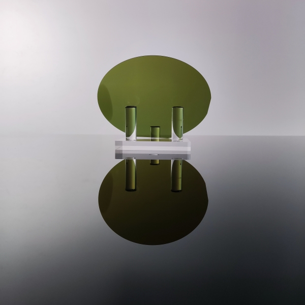
Below is a snapshot of the referenced research paper“Quantum enhanced electric field mapping within semiconductor devices”. If you are interested in this study or wish to learn more about our products, feel free to contact us!
As semiconductor technology advances, Gallium Nitride (GaN) has become a core material in optoelectronics, rad...
With the rapid advancement of third-generation semiconductor technologies, Silicon Carbide (SiC) has emerged a...
As third-generation semiconductor materials such as silicon carbide (SiC) and gallium nitride (GaN) continue t...