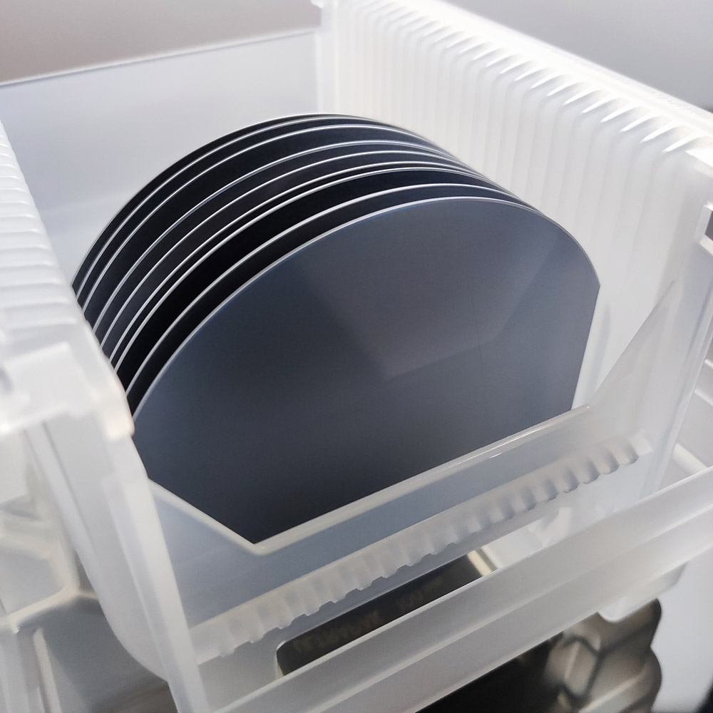
Gallium nitride (GaN) on silicon is a promising semiconductor material that combines the unique electrical and optical properties of GaN with the low cost and high scalability of silicon substrates. In this article, we will discuss the performance characteristics and potential applications of GaN on silicon growth.

One of the key advantages of GaN on silicon is its high electron mobility, which allows for high-speed electronic devices with low power consumption. Additionally, GaN on silicon has a high thermal conductivity, which makes it suitable for applications that require efficient heat dissipation.
Another important property of GaN on silicon is its high optical transparency, which makes it ideal for optoelectronic applications such as light-emitting diodes (LEDs) and photovoltaic cells. GaN on silicon has a wide bandgap, which allows for efficient light emission and absorption in the ultraviolet, visible, and infrared regions of the electromagnetic spectrum.
GaN on silicon also has excellent mechanical properties, including high hardness and strength, as well as a low coefficient of thermal expansion. This makes it suitable for a wide range of structural applications that require high strength and durability.
The growth of GaN on silicon is typically achieved through metal-organic chemical vapor deposition (MOCVD) or molecular beam epitaxy (MBE) techniques. These techniques allow for precise control of the growth process and the resulting material properties.
Some of the potential applications of GaN on silicon include high-speed electronic devices such as power amplifiers and transistors, as well as optoelectronic devices such as LEDs, lasers, and photovoltaic cells. GaN on silicon is also being explored for use in high-temperature applications such as power electronics, as well as for structural components in aerospace and defense applications.
In conclusion, GaN on silicon is a highly promising material with a unique combination of electrical, optical, and mechanical properties. As research into this material continues, it is likely to find a growing number of applications in a variety of industries, from electronics to aerospace and beyond. The scalability and cost-effectiveness of silicon substrates make GaN on silicon an attractive option for a wide range of applications.
Related product links
Silicon Carbide (SiC) Substrate
As semiconductor technology advances, Gallium Nitride (GaN) has become a core material in optoelectronics, rad...
With the rapid advancement of third-generation semiconductor technologies, Silicon Carbide (SiC) has emerged a...
As third-generation semiconductor materials such as silicon carbide (SiC) and gallium nitride (GaN) continue t...