GaN on Silicon:
● Typical Structure: ● Typical Specification:
1.undoped GaN GaN layer thickness up to 7μm on silicon(111)
2.n-type GaN(Si-doping) GaN layer thickness up to 7μm on silicon(111)
3.HEMT structures HEMT structure on silicon
4.LED structures LED structure (400-520nm wavelength) on silicon
● Specifications for GaN-HEMT-on-Si Epi-wafers:
Wafer Size: 200mm
Substrate: p-type Si(111)
Substrate Thickness: 1000±25μm
GaN Cap: 2 ~ 3 nm
AlGaN barrier: 20 ~ 25 nm, 20% - 25% Al
AlN spacer: ~ 1 nm, Optional
GaN Channel: > 150 nm
Buffer: > 3.5 μm
2DEG density*: > 9E12/cm²
Electron mobility*: > 1500 cm2/Vs
Sheet resistance: < 400 Ω/□
Buffer resistivity: > 105 (Ω·cm)
Vertical Breakdown: > 600V @ 1mA/cm²
Wafer bow / Warp: < 50 μm
Surface morphology: rms < 0.5 nm in 5 × 5 μm²
● Specidfications for Blue GaN-on-Si LED Epi-wafers:
Wafer Size: 4"/6"/8"
Substrate: Si(111)
Substrate Thickness: 800μm/1mm/1.15 mm
P-(AlIn)GaN: 120 - 170 nm, [Mg] > 1E19/cm3
InGaN/GaN Multiple Quantum Wells: 100 - 200 nm
nGaN: 1.40 - 1.60 μm, [Si] ~ 5.0E18/cm³
Buffer: 1.50 - 1.70 μm
Average Dominant Wavelength: 450 ~ 470 nm
Wafer bow: < ±50 μm
FWHM: < 20 nm
● Reference:
2"/ 4"/6"/8" Silicon substrate is available.
Up to 7µm GaN epitaxial layer on Silicon
RMS(AFM)<0.5nm
CC < 1E17/cm³
AlN and AlGaN buffer layers used in order to relax GaN
Thickness uniformity < 5%
Wafer Bow<50μm
● Epitaxial structure and substrate specifications can be customized,anna@jxtwafer.com
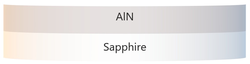
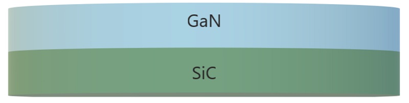
● Epitaxy structure:
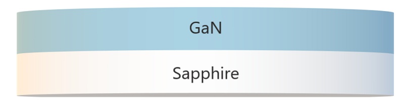
● Advantages: low cost, good stability in high temperature, excellent mechanical properties, mature technology in LED field.
● Disadvantages: low thermal conductivity, the lattice mismatch in power devices, a little worse performance.
● Application:used in LED and optoelectronic fields.
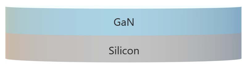
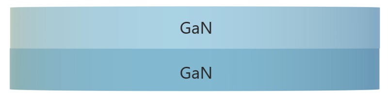
● Epitaxy structure:
● Advantages: low price of the substrates, good electrical and thermal conductivity, large-scale industrialization.
● Disadvantages: the lattice parameters of sillicon aren't matched to GaN very well , resulting in slightly poor wafer performance and low yield.
● Application: used in HEMT and chips for consumer electronics , RF chips,etc.
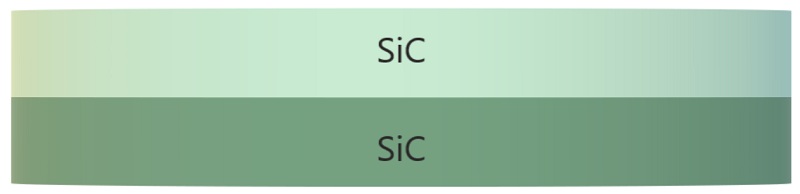
● Epitaxy structure:
● Advantages: high temperature resistance, low loss, excellent performance.
● Disadvantages: limited supply of gallium nitride substrates, complicated technology, high cost, and low-scale industrialization.
● Application: used in blue light, green laser and other optoelectronic fields.
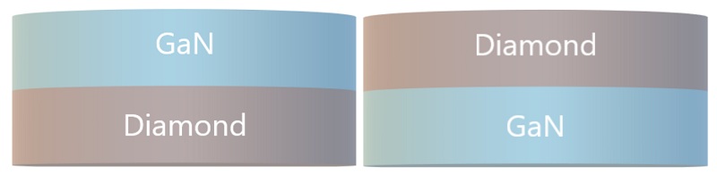
● Epitaxy structure:
● Advantages: high thermal conductivity, good antistatic ability, excellent performance.
● Disadvantages: poor machining performance, high cost, limited application scenarios.
● Application: used in 5G base station RF chips, satellite radar, LED and optoelectronic fields.
If you want to know more epitaxial structures, please email us anna@jxtwafer.com.