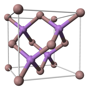
Gallium Arsenide (GaAs), with the chemical formula GaAs, is a black-gray solid with a melting point of 1238°C. It remains stable in air at temperatures below 600°C and is resistant to corrosion by non-oxidizing acids.
Gallium arsenide is a crucial semiconductor material classified as a III-V compound semiconductor. It crystallizes in a zinc blende lattice structure, with a lattice constant of 5.65×10⁻¹⁰ m and a melting point of 1237°C. The material has a bandgap energy of 1.4 eV. Gallium arsenide became commercially viable in 1964. It can be fabricated into semi-insulating high-resistance materials with resistivity three orders of magnitude higher than that of silicon or germanium, making it ideal for use as substrates in integrated circuits, infrared detectors, and gamma photon detectors. Due to its electron mobility being 5 to 6 times greater than that of silicon, gallium arsenide is widely used in the fabrication of microwave devices and high-speed digital circuits. Semiconductor devices made from gallium arsenide exhibit superior performance in high-frequency, high-temperature, and low-temperature conditions, along with low noise and strong radiation resistance. Additionally, it is suitable for the production of transfer devices such as bulk effect devices. Gallium arsenide is a semiconductor material that combines multiple advantages, but transistors made from it have a low amplification factor and poor thermal conductivity, making them less suitable for high-power applications. Although gallium arsenide offers exceptional performance, its tendency to decompose at high temperatures makes the production of high-purity single-crystal materials with an ideal chemical composition technically challenging.
The CAS number for gallium arsenide (Gallium arsenide, ヒかガリウム) is 1303-00-0. Typically, gallium arsenide crystallizes in a cubic zinc blende structure (as shown in Figure 1), with a space group of F-43m.

1. Gallium arsenide is a compound semiconductor material extensively used in transistors, lasers, solar cells, and various high-speed integrated circuit chips.
2. Gallium arsenide appears as a bright gray substance with a metallic luster. It is brittle and hard, with a density of 5.316 g/cm³, a melting point of 1227°C, and a Mohs hardness of 4.5. It is relatively stable at room temperature, does not react with hydrochloric acid, sulfuric acid, or hydrofluoric acid, but can react with concentrated nitric acid, as well as with hot hydrochloric acid and sulfuric acid.
3. Gallium arsenide is a direct bandgap semiconductor with a bandgap energy of 1.4 eV at room temperature. Its lattice constant is 5.653 Å, the high-frequency dielectric constant is 11.1, and the effective electron mass is 0.067. The material exhibits anisotropic effective masses for light and heavy holes, with values of 0.34 and 0.09, respectively, along the [100] crystal direction. At room temperature, the electron and hole mobilities are 3300 cm²/Vs and 400 cm²/Vs, respectively.
4. At room temperature, gallium arsenide has a thermal conductivity of 0.56 W/cm·K and a Debye temperature of 344 K.
5. Gallium arsenide is typically doped with silicon to form n-type semiconductors and with zinc to form p-type semiconductors. Currently, single-crystal gallium arsenide wafers are available in diameters ranging from 1 inch to 12 inches.
Synthesis Method
The preparation apparatus for gallium arsenide is shown in the figure. First, a quartz disk containing pure gallium is placed in a transparent quartz ampoule, sealed at one end, followed by the addition of pure arsenic. The ampoule is then vacuum-sealed at 5×10⁻⁶ Torr (1 Torr = 133.322 Pa). The amount of arsenic added should be 1.1 to 1.2 times its stoichiometric equivalent (since the vapor pressure of arsenic is controlled, the amount added must slightly exceed that needed to fill the entire ampoule). To prevent gallium arsenide and the disk from absorbing moisture, the disk must be sandblasted about 150-300 times. The ampoule is then set up as shown, with the furnace containing arsenic heated to 610°C and the furnace containing gallium heated to 1250°C (depending on the size of the ampoule, arsenic is added at 1.1 to 1.2 times its molar amount).
At 610°C, the vapor pressure of arsenic is 101.325 kPa, and it reacts with gallium heated to 1250°C to produce gallium arsenide. After 4-5 hours, the ampoule is drawn out of the furnace containing arsenic by 5-20 mm every hour, gradually growing a single crystal from the front end of the disk.
Main Applications
Gallium arsenide is used in the manufacture of optoelectronic devices (LCDs), lasers (LDs), field-effect transistors (FETs), high-electron-mobility transistors (HEMTs), heterojunction bipolar transistors (HBTs), high-speed devices, and microwave monolithic integrated circuits (MMICs), microwave/millimeter-wave integrated circuits (MIMICs), high-speed integrated circuits, and solar cells.
Properties and Stability
When used and stored according to specifications, gallium arsenide does not decompose, and no known hazardous reactions occur. It should be kept away from acids and moisture/humidity.
As a compound semiconductor, gallium arsenide emits light directly when current passes through the p-n junction, making it suitable for use in lasers and light-emitting diodes. Additionally, it can be used as a functional component in microwave oscillation, millimeter-wave amplification, and optical communications.
As semiconductor technology advances, Gallium Nitride (GaN) has become a core material in optoelectronics, rad...
With the rapid advancement of third-generation semiconductor technologies, Silicon Carbide (SiC) has emerged a...
As third-generation semiconductor materials such as silicon carbide (SiC) and gallium nitride (GaN) continue t...
