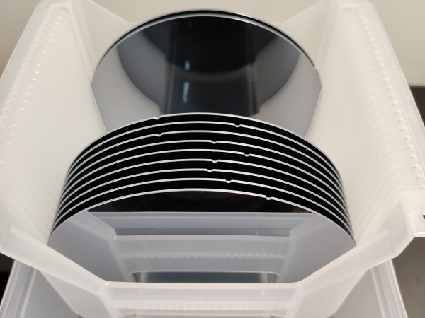
In semiconductor manufacturing, wafer substrates serve as the fundamental material for integrated circuits (ICs), optoelectronic devices, and power electronics. Precise alignment is crucial during fabrication, and the industry employs two primary identification methods: flat edges (Flat) and notches (Notch). These markers indicate crystallographic orientation and doping type, ensuring proper positioning in semiconductor processes.
Why do some wafers use Flat edges while others adopt Notches? This article explores the evolution, technical distinctions, and applications of these two marking methods.
1. Technical Comparison of Flat vs. Notch
1.1. Flat Edge (Flat)
The Flat method involves cutting one or more straight edges along the wafer’s perimeter, primarily used for wafers ≤6 inches in size. The main functions of Flat markers include:
Indicating crystal orientation, such as <100> or <111>, to ensure accurate processing;
Distinguishing doping types (P-type or N-type);
Providing manual or semi-automated alignment cues, particularly for early-generation lithography and etching equipment.
Different doping types and crystal orientations in silicon (Si) wafers correspond to distinct Flat configurations:
P-type <100> wafer: One large Flat;
N-type <100> wafer: One large Flat + one small Flat;
P/N-type <111> wafer: One large Flat only.
Although this marking system was widely used in early semiconductor processing, its limitations became evident as wafer sizes increased.
1.2. Notch
A Notch is a small V-shaped or U-shaped groove positioned on the wafer’s edge, typically at 180°. Notches are predominantly used in 8-inch and larger silicon wafers, offering several advantages:
Better compatibility with automation: Notches facilitate faster and more precise alignment in automated processing equipment.
Minimized edge stress concentration: Compared to Flat edges, Notches reduce mechanical stress on the wafer perimeter, improving structural integrity.
Standardization: As 8-inch and larger wafers became industry norms, SEMI (Semiconductor Equipment and Materials International) mandated Notches for these wafer sizes, ensuring process consistency.
Today, 8-inch, 12-inch, and larger wafers almost exclusively use Notches, while wafers ≤6 inches still predominantly use Flats.
2. Evolution and Adoption of Flat vs. Notch
2.1. Why Early Wafers Used Flat Markers
During the 1970s to 1990s, semiconductor wafers were primarily 2-inch, 3-inch, 4-inch, and 6-inch in diameter. At the time, semiconductor processing equipment relied on manual or optical alignment, where Flat markers provided an intuitive reference for technicians. Consequently, Flat edges became the industry standard.
Additionally, compound semiconductors (e.g., SiC, GaN, and sapphire) have higher hardness, making Notch cutting more challenging. As a result, Flat markers remained the preferred choice.
2.2. The Rise and Standardization of Notch Markers
With the introduction of 8-inch wafers in the 1990s, the semiconductor industry shifted toward full automation. Lithography, etching, and ion implantation processes required high-precision mechanical alignment, where Notches provided a more reliable and less intrusive marking method.
Today, 12-inch and larger wafers universally adopt Notches, and some 8-inch SiC wafers are also transitioning to Notches for enhanced automation compatibility.
3. Marking Methods for Different Semiconductor Materials
The choice between Flat and Notch markers depends on the material's physical properties and manufacturing requirements:
| Material | Common Sizes | Marking Method | Reason |
| Silicon (Si) | 2” - 6” | Flat | Traditional method, suitable for manual/semi-automated processes |
| Silicon (Si) | 8” - 12” | Notch | Optimized for automation, SEMI industry standard |
| Silicon Carbide (SiC) | 2” - 6” | Flat | High mechanical hardness, traditional processing method |
| Silicon Carbide (SiC) | 8” | Notch(partial adoption) | Emerging standard for automated processing |
| Gallium Nitride (GaN) | 2” - 6” | Flat | Determined by substrate type (SiC, sapphire, etc.) |
| Sapphire (Al₂O₃) | 2” - 8” | Flat | Extremely high hardness, Notch cutting is difficult |
From this comparison, it is evident that silicon wafers ≥8 inches exclusively use Notches, whereas SiC, GaN, and sapphire substrates still primarily use Flat markers. However, as processing technologies evolve, SiC wafers may gradually transition to Notch-based marking to enhance automation compatibility.
4. Conclusion
Flat and Notch markers have evolved alongside semiconductor wafer sizes and manufacturing techniques. Flat markers remain dominant in smaller wafers, especially for materials where manual or semi-automated processing is common. In contrast, Notches are now the standard for 8-inch and larger silicon wafers, offering superior alignment precision in automated production environments.
As semiconductor technology advances, SiC wafers (particularly 8-inch variants) may increasingly adopt Notch markers to facilitate automation. However, in materials with extreme hardness (such as sapphire), Flat markers are expected to remain the industry norm.
For wafer manufacturers and equipment suppliers, understanding the differences between Flat and Notch markers is essential for optimizing production efficiency and ensuring compatibility with modern semiconductor fabrication processes.
If you require high-quality SiC, GaN, or sapphire wafers, JXT Technology Co., Ltd. offers premium semiconductor substrates and customized solutions. Contact us today to learn more.
As semiconductor technology advances, Gallium Nitride (GaN) has become a core material in optoelectronics, rad...
With the rapid advancement of third-generation semiconductor technologies, Silicon Carbide (SiC) has emerged a...
As third-generation semiconductor materials such as silicon carbide (SiC) and gallium nitride (GaN) continue t...