With the rapid advancement of third-generation semiconductor technology, silicon carbide (SiC) wafers have become a core material in power electronics, RF devices, and semiconductor applications due to their superior high-temperature, high-voltage, and high-frequency performance. Today, we will provide a concise introduction to the SiC wafer manufacturing process, accompanied by a visual diagram for better understanding.
SiC Wafer Manufacturing Process
The fabrication of SiC wafers primarily involves the following five key steps:
1. Silicon Carbide Seed (SiC Seed)
The SiC wafer growth process begins with a high-quality SiC seed crystal that serves as the foundation for growing SiC ingots. The quality and crystallographic orientation of this seed crystal play a crucial role in determining the final properties of the SiC ingot.
2. Growth of Silicon Carbide Ingot (SiC Ingot)
SiC ingots are grown using either the Physical Vapor Transport (PVT) method or Chemical Vapor Deposition (CVD). In this process, silicon and carbon vapor-phase compounds deposit onto the seed crystal at high temperatures (around 2000°C) and under controlled low-pressure conditions, gradually forming large SiC ingots. Precise control over this growth process is essential to ensure high crystalline quality with minimal defects.
3. Ingot Slicing (Slicing)
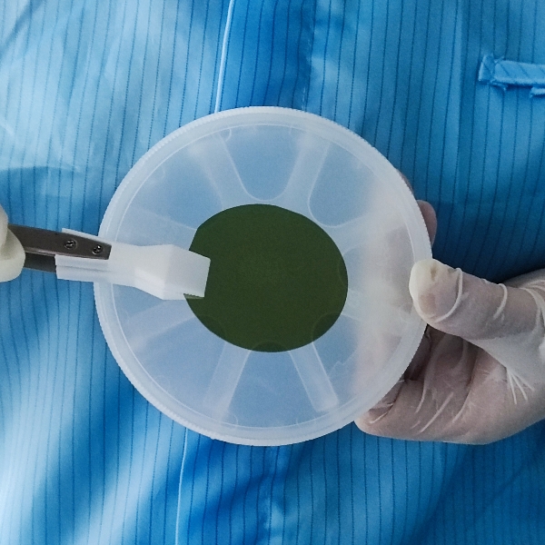
Once the SiC ingot reaches the desired size, it is sliced into thin wafers using diamond wire sawing technology. Due to the extreme hardness of SiC (second only to diamond), high-precision cutting equipment and appropriate cooling techniques are required to minimize material loss and improve wafer surface quality.
(The following image illustrates the entire SiC wafer manufacturing process)
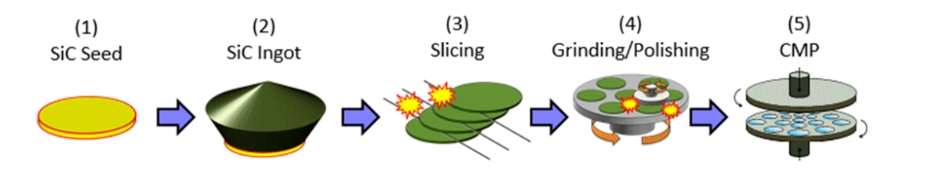
4. Grinding and Polishing (Grinding/Polishing)
After slicing, the surface of the SiC wafer remains relatively rough and must undergo mechanical grinding and polishing to enhance surface flatness and reduce microscopic defects. This process typically involves multiple stages of fine machining using diamond abrasives.
5. Chemical Mechanical Polishing (CMP)
Chemical Mechanical Polishing (CMP) is a critical step in SiC wafer fabrication. It combines chemical etching with mechanical polishing, effectively removing surface imperfections and achieving a mirror-like finish. This process is particularly vital for high-quality SiC substrates, as it directly affects the growth quality of subsequent epitaxial layers.
Key Advantages of SiC Wafers
Compared to traditional silicon (Si) wafers, SiC wafers offer numerous advantages, including:
✅ High-temperature resistance (operating temperatures exceeding 600°C)
✅ High breakdown electric field strength (10 times that of silicon, ideal for high-voltage power devices)
✅ Superior thermal conductivity (enhanced heat dissipation for improved device stability)
✅ Excellent high-frequency performance (suitable for 5G communication and RF power amplifiers)
Due to these exceptional properties, SiC wafers are widely used in electric vehicles (EVs), industrial power supplies, RF communication systems, satellite electronics, and solar inverters, among other advanced applications.
Conclusion
The manufacturing of SiC wafers is a highly sophisticated and precision-driven process, with each step impacting the final device performance and reliability. As SiC technology continues to advance, we anticipate that SiC wafers will play an increasingly pivotal role in the semiconductor industry, driving innovations toward higher efficiency and greater sustainability.
If you are interested in SiC wafers or related products, JXT Technology Co., Ltd. offers high-quality SiC substrates and epitaxial solutions tailored to your needs.
As semiconductor technology advances, Gallium Nitride (GaN) has become a core material in optoelectronics, rad...
With the rapid advancement of third-generation semiconductor technologies, Silicon Carbide (SiC) has emerged a...
As third-generation semiconductor materials such as silicon carbide (SiC) and gallium nitride (GaN) continue t...