In the realm of semiconductor materials, epitaxial growth stands as a pivotal technique, enabling precise control over crystal structures and properties. This method not only plays a crucial role in semiconductor fabrication but also drives innovation across various industries.
What is Epitaxial Growth?
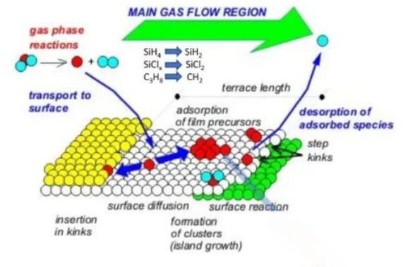
Epitaxial growth is a process wherein atoms or molecules are deposited on the surface of a crystal, gradually increasing its size. In the semiconductor field, epitaxial growth often occurs on the surface of an epi wafer, allowing for precise control of growth conditions to ensure the newly grown crystal maintains the structure and orientation of the underlying substrate. This method is essential for producing semiconductor materials with specific performance and functionality.

Why Epitaxial Growth is Essential?
In the semiconductor industry, epitaxial growth is indispensable for several reasons:
1. Precise Control of Material Structure: Epitaxial growth techniques enable precise control over crystal orientation, thickness, and shape. This level of precision is vital for fabricating high-performance devices on epi wafers.
2. Multi-Layered Structures: By employing various materials in epitaxial growth on SiC epi/epitaxial wafers, complex multi-layered structures can be created. This capability is crucial for the development of integrated circuits and optoelectronic devices.
3. Enhanced Crystal Quality: Epitaxial growth often results in crystals with low defect densities and high crystalline quality, enhancing device performance and stability on SiC epi/epitaxial wafers.
4. Directional Growth: Epitaxial growth allows for directional growth, facilitating the formation of specific device structures on epi wafers.
Classification of Epitaxial Growth
In the semiconductor field, epitaxial growth can be classified into several types based on methods and conditions:
1. Vapor Phase Epitaxy (VPE):
Applications: Widely used in semiconductor and optoelectronic device fabrication, such as LEDs, laser diodes, and solar cells on epi wafers.
Advantages: High-quality, uniform crystals suitable for multi-layered structures and complex devices on SiC epi/epitaxial wafers.
2. Liquid Phase Epitaxy (LPE):
Applications: Commonly applied in photonics, sensors, and communication devices, such as infrared detectors and optical communication devices on epi wafers.
Advantages: Large-area, low-defect density crystals, particularly suitable for specific material systems on SiC epi/epitaxial wafers.
3. Molecular Beam Epitaxy (MBE):
Applications: Utilized for high-performance semiconductor research and quantum devices, offering atomic-level control and the production of ultra-thin films and high-quality crystals on epi wafers.
Advantages: Precision control at the atomic level, facilitating the growth of ultra-thin films and high-quality crystals on SiC epi/epitaxial wafers.
4. Solid Phase Epitaxy (SPE):
Applications: Used for thin film, multi-layered structures, and semiconductor device fabrication, providing advantages in low-temperature growth and sensitive materials on epi wafers.
Advantages: Low-temperature growth suitable for temperature-sensitive materials on SiC epi/epitaxial wafers.
5. Step Flow Epitaxy:
Applications: Employed in the fabrication of complex multi-layered structures and specialized nanostructures, offering precise control over growth rates and layers on epi wafers.
Advantages: Control over growth rates and layering, suitable for forming specific shapes and sizes on SiC epi/epitaxial wafers.

Conclusion
In conclusion, epitaxial growth techniques in semiconductor materials represent a crucial aspect of fabrication technology. Through various types of epitaxial growth, precise control over crystal structures, properties, and device functionalities can be achieved on epi wafers. Each epitaxial type finds its niche in specific application areas on SiC epi/epitaxial wafers, providing distinct advantages that propel the semiconductor industry forward in innovation and development.
As semiconductor technology advances, Gallium Nitride (GaN) has become a core material in optoelectronics, rad...
With the rapid advancement of third-generation semiconductor technologies, Silicon Carbide (SiC) has emerged a...
As third-generation semiconductor materials such as silicon carbide (SiC) and gallium nitride (GaN) continue t...
