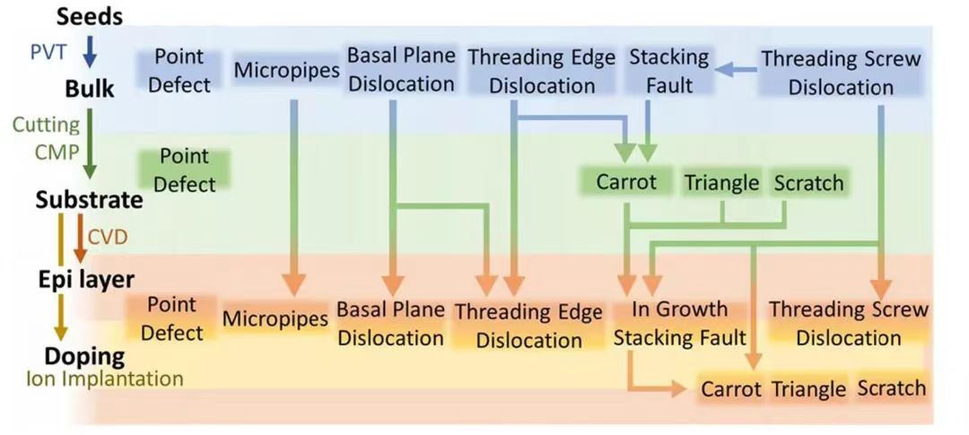
Silicon carbide (SiC) serves as a crucial semiconductor material with wide applications in power electronics, optoelectronics, and various other fields. However, during the growth process of SiC, various defects often arise, significantly impacting the material's performance and device reliability. Hence, understanding the types of these defects, detection methods, and approaches for enhancing SiC quality is paramount.
Types of Defects:
1. Dislocations:
Dislocations, including line and point defects within the crystal lattice, affect the material's electrical and mechanical properties.
2. Grain Boundaries:
Interfaces between crystal grains, known as grain boundaries, may influence the material's electrical properties and stability.
3. Point Defects:
Point defects, such as vacancies, interstitials, and impurities, can impact the material's electrical and optical properties.
4. Polytype Variations:
SiC can exist in different polytypes like 4H-SiC and 6H-SiC, and transitions between these polytypes may affect material properties.
5. Inhomogeneous Grain Size and Distribution:
Variations in grain size and distribution can lead to differences in material properties.
6. Presence of Impurities:
Impurities like oxygen, nitrogen, and aluminum may affect the material's electrical properties and stability.

Detection Methods:
Transmission Electron Microscopy (TEM):
Used to observe crystal structure and defects like dislocations.
Scanning Electron Microscopy (SEM):
Used for examining surface morphology and grain size distribution.
Raman Spectroscopy:
Utilized for analyzing crystal structure and point defects.
X-ray Diffraction (XRD):
Applied for determining crystal structure and grain orientation.
Methods for Quality Enhancement:
Optimization of Growth Processes:
Adjusting growth parameters to minimize defect formation.
Control of Growth Conditions:
Regulating growth temperature, atmosphere, etc., to promote crystal growth and defect repair.
Selection of Suitable Substrate Materials:
Companies like JXT provide high-quality silicon carbide substrates in various models (Silicon Carbide Wafer and SiC substrate). JXT's experience highlights the importance of providing high-quality substrates for the overall quality of SiC materials and devices. Ensuring the availability of different substrate models caters to diverse application needs.
Post-Growth Material Treatments:
Employing post-growth treatments like annealing, surface treatments, etc., to reduce defects and enhance material quality.
In conclusion, understanding defects during SiC growth, employing suitable detection methods, and adopting comprehensive approaches to enhance SiC quality are essential for advancing SiC material applications. Insights from JXT Company underscore the significance of providing high-quality SiC substrates for ensuring the overall quality of SiC materials and devices.
As semiconductor technology advances, Gallium Nitride (GaN) has become a core material in optoelectronics, rad...
With the rapid advancement of third-generation semiconductor technologies, Silicon Carbide (SiC) has emerged a...
As third-generation semiconductor materials such as silicon carbide (SiC) and gallium nitride (GaN) continue t...
