At present, silicon carbide accelerates penetration in new energy, charging piles, rail transit and other fields. Moreover, due to its high-speed switching and low on-resistance characteristics, it can exhibit excellent electrical characteristics even under high temperature conditions, greatly reducing switching losses, making components smaller and lighter, more efficient in performance, and improving the overall reliability of the system.
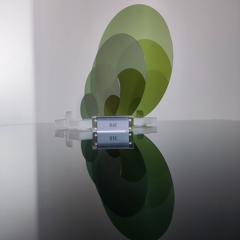
JXT Technology Co.,Ltd. have been developing SiC wafers. Now JXT can offer 2inch, 4inch, 6inch, 8inch SiC wafers stably.

1.Properties
Band Gap(eV):3.26
Breakdown Electrical Field (MV/cm):3.1
Thermal Conductivity(W/cm.K):3.7-4.9
Thermal Expansion :4.7*10-6/k
Refractive Index :2.6767~2.6480
Saturation Drift Velocity(m/s):2.0×105
2. 8 inch 4H-N SiC wafers Specification
Diamater: 200±0.5mm
Thickness:500±25μm
Surface Orientation: Off-Axis:4°toward <11-20>±0.5°
Notch Orientation: [1-100]±1.0°
Resistivity: 0.015-0.028 Ω.cm
Si Face: CMP
C Face: MP
TTV≤ 15
Bow≤ 20
Wrap ≤ 20
LTV ≤ 20
3. Application
Silicon carbide wafers are used in photovoltaic inverter power supplies, new energy electric vehicles and charging piles, smart grids, high-frequency electric welding, rail transit, industrial control special power supplies, national defense and military industries, etc.
As third-generation semiconductor materials such as silicon carbide (SiC) and gallium nitride (GaN) continue t...
With the continuous advancement of power electronics, RF devices, and optoelectronic technologies, the demand ...
The selection of substrate materials plays a crucial role in the development of high-frequency, high-power RF ...