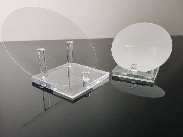
Chemical Mechanical Polishing (CMP) is a surface planarization technique that combines chemical etching and mechanical abrasion, widely used in semiconductor manufacturing. The CMP process uses chemical polishing slurry containing etchants that react with the wafer surface material, making it easier to abrade. Simultaneously, abrasive particles in the slurry, under mechanical pressure, perform physical abrasion on the wafer surface through rotation and relative motion. This process not only achieves nanoscale surface flatness but also effectively removes excess material, making it a high-precision, high-efficiency surface treatment method. CMP is extensively applied in areas such as multi-layer metal interconnects, thin-film transistors, and flexible electronic devices, making it a critical process in modern semiconductor manufacturing.

Why Use CMP for Wafer Substrate Planarization?
The application of CMP in wafer substrate planarization offers numerous advantages and necessities. Firstly, CMP significantly enhances the flatness of the wafer surface, which is fundamental for achieving multi-layer interconnect technology. In semiconductor device fabrication, each metal and dielectric layer requires a flat surface to ensure the precise execution of subsequent process steps such as photolithography and etching. A flat surface can reduce optical distortion, ensuring accurate pattern transfer and improving circuit performance.
Secondly, the application of CMP can improve the electrical performance of devices. A flat surface ensures uniformity in material deposition and etching processes, thereby enhancing device consistency and reliability. By reducing material buildup and recesses, CMP can prevent electrical short circuits and open circuits. Additionally, CMP's precise control over material removal allows it to adapt to the needs of various process steps, enhancing process compatibility and flexibility.
Moreover, CMP facilitates the development of advanced manufacturing technologies. In 3D integrated circuits and system-in-package (SiP) technologies, a flat wafer surface is crucial for achieving high-density vertical interconnects. For ultra-thin wafers and films, planarization is essential for ensuring mechanical stability and electrical performance. By eliminating surface non-uniformities, CMP can significantly reduce processing defects and increase yield.
In summary, CMP improves the flatness of the wafer surface, enhancing the reliability and precision of subsequent processes and improving the electrical and mechanical properties of devices. It is a key process for achieving high-performance and high-density integrated circuit manufacturing. The high precision, efficiency, and broad applicability of CMP make it an indispensable technology in semiconductor manufacturing.
Related product links
As semiconductor technology advances, Gallium Nitride (GaN) has become a core material in optoelectronics, rad...
With the rapid advancement of third-generation semiconductor technologies, Silicon Carbide (SiC) has emerged a...
As third-generation semiconductor materials such as silicon carbide (SiC) and gallium nitride (GaN) continue t...
