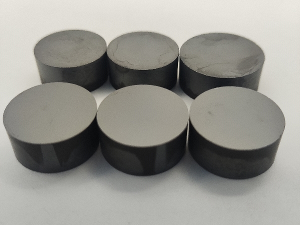
Silicon carbide (SiC) substrates play a crucial role in the semiconductor industry, particularly in high-temperature, high-power, and high-frequency applications. Their exceptional electrical and thermal properties make them ideal for high-performance electronic devices. The processing of SiC substrates is complex, with grinding and polishing processes being particularly critical as they directly impact the yield and performance of subsequent device manufacturing. This article focuses on the technical analysis of the grinding and polishing processes for SiC substrates.
1. Grinding
Grinding is the first step in the planarization process, primarily aimed at removing the rough surface and thickness irregularities caused by the slicing process. Diamond grinding wheels with coarse abrasives are typically used for mechanical grinding. Due to the extremely high hardness of SiC, grinding can easily introduce cracks and damage layers, necessitating careful control of grinding parameters. Proper cooling and grinding speeds are essential to minimize damage.
2. Fine Grinding
Following coarse grinding, fine grinding further reduces surface damage and improves flatness. This step uses finer diamond abrasives for grinding, striking a balance between flatness and processing efficiency. Although fine grinding significantly enhances surface quality, it may still leave minor damage that requires further treatment.
3. Chemical Mechanical Polishing (CMP)
CMP is the most critical step in the planarization process of SiC substrates, aiming to achieve nanoscale surface flatness and smoothness while removing minor damage caused by mechanical processing. CMP combines chemical corrosion and mechanical grinding, softening the surface material through chemical reactions, followed by mechanical removal of the softened layer.
Polishing Slurry: Commonly used polishing slurries contain oxidants and corrosives, such as hydrogen peroxide and alkaline solutions. The choice of chemical components is crucial to ensure the material removal rate and surface quality.
Polishing Pad: The selection of polishing pads with appropriate hardness and material is essential to optimize the material removal rate and surface quality. Excessive or insufficient hardness can negatively impact polishing results.
Process Control: Balancing the rates of chemical reaction and mechanical removal is key in CMP. Too rapid a chemical reaction can cause surface corrosion, while excessive mechanical removal may introduce new defects.
4. Quality Inspection
To ensure the flatness and smoothness of SiC substrates, a series of quality inspections are conducted.
Optical Inspection: Microscopes and interferometers are used to detect surface flatness and microscopic defects.
Atomic Force Microscopy (AFM): Employed for high-resolution measurement of surface roughness.
X-Ray Diffraction (XRD): Used to assess the integrity and stress distribution of the crystal structure.

Technical Challenges and Solutions
1. Processing High-Hardness Material:
Challenge: The high hardness of SiC makes mechanical processing difficult and prone to damage.
Solution: Use high-quality diamond grinding wheels and optimized grinding parameters, with proper control of cooling and grinding speeds.
2. Surface Damage and Cracks:
Challenge: Coarse and fine grinding can introduce microcracks and damage layers.
Solution: Employ multi-step grinding and polishing processes to gradually reduce damage, optimizing processing parameters at each step.
3. Polishing Uniformity:
Challenge: Achieving uniformity during CMP is difficult, often leading to surface unevenness.
Solution: Optimize polishing slurry formulation and pad selection, precisely control CMP process parameters, and conduct multi-point uniformity checks.
Future Development Directions
With the increasing demand for high-power, high-frequency, and high-temperature electronic devices, the grinding and polishing processes for SiC substrates are continually evolving. Future directions include:
Efficient CMP Technology: Developing more efficient CMP processes to reduce surface damage and increase polishing speed.
Advanced Surface Inspection Technology: Introducing more advanced surface inspection technologies, such as online AFM and real-time optical inspection, to enhance inspection accuracy and efficiency.
Automation and Intelligence: Utilizing automated equipment and intelligent control systems to optimize grinding and polishing processes, minimizing human factors.
By continuously optimizing grinding and polishing processes, the surface quality of SiC substrates can be further improved, thereby enhancing their application in high-performance electronic devices.
As semiconductor technology advances, Gallium Nitride (GaN) has become a core material in optoelectronics, rad...
With the rapid advancement of third-generation semiconductor technologies, Silicon Carbide (SiC) has emerged a...
As third-generation semiconductor materials such as silicon carbide (SiC) and gallium nitride (GaN) continue t...
