Introduction
Sapphire substrates are widely used in optoelectronics and semiconductor industries due to their exceptional mechanical strength, thermal stability, and optical properties. In recent years, with the rapid development of LED, micro-LED, and compound semiconductor technologies, Nano-patterned Sapphire Substrates (NPSS) have gained significant attention for their ability to enhance the crystal quality of epitaxial materials and improve light extraction efficiency.
Features of NPSS Technology
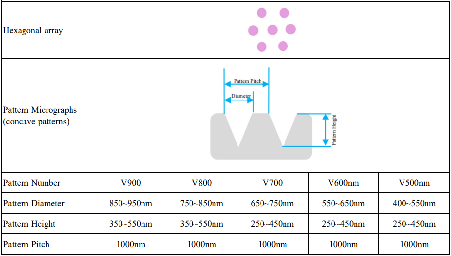
NPSS is fabricated by employing advanced photolithography and etching techniques to form periodic nano-structures (typically hexagonal arrays of concave or convex patterns) on the sapphire substrate surface. Compared with conventional planar sapphire substrates, NPSS offers several technical advantages:
1. High-Purity Material
NPSS substrates are made from >99.99% high-purity single-crystal sapphire, usually grown using the Kyropoulos method. This ensures excellent chemical stability during high-temperature epitaxial processes.
2. Precision Pattern Structures
The surface patterning of NPSS features high precision:
Pattern Array: Hexagonal arrangement.
Pattern Size: Available in various diameters (e.g., 850–950 nm) and heights (e.g., 350–550 nm).
Pitch: Typically 1000 nm.
These structures are optimized to significantly reduce defect density during epitaxial growth.
3. Epi-Ready Surface
The front surface of NPSS undergoes fine polishing to achieve an Epi-ready standard, ensuring surface roughness below 1 nm and making it suitable for direct epitaxial applications.
4. Customizability
NPSS offers multiple specifications (e.g., V900, V800), allowing users to select appropriate pattern sizes and heights based on specific epitaxial requirements.

Technical Advantages of NPSS
1. Improved Crystal Quality of Epitaxial Layers
The surface patterns of NPSS help alleviate stress caused by lattice mismatches during epitaxial growth, effectively reducing dislocation density. This is particularly beneficial for compound semiconductors like GaN, significantly enhancing the quality of the epitaxial layers.
2. Enhanced Light Extraction Efficiency
Patterned structures minimize total internal reflection, allowing more light to escape through the substrate surface, thereby improving light extraction efficiency. This is critical for high-brightness LEDs and micro-LEDs.
3. Reduced Production Costs
With improved light extraction efficiency, LED devices can achieve the same brightness at lower current levels, reducing power consumption and heat dissipation requirements.
Major Application Areas of NPSS
1. High-Brightness LEDs (HB-LEDs)
NPSS is widely used in the LED industry. By incorporating NPSS in blue or white LED epitaxy, light efficiency and device reliability can be significantly enhanced.
2. Micro-LED Display Technology
Micro-LEDs are the core of next-generation display technology due to their high brightness, low power consumption, and long lifespan. The precise pattern structures of NPSS make it ideal for the high-precision requirements of micro-LED epitaxial growth.
3. Compound Semiconductor Devices
NPSS is commonly used for the epitaxial growth of GaN, AlN, and other compound semiconductors, supporting the production of power devices and laser diodes. Its ability to reduce dislocation density significantly improves device performance.
4. Optical and Infrared Window Materials
The high-purity sapphire material and patterned surface of NPSS are also suitable for specific optical lenses and window applications, especially in scenarios requiring high transmittance and durability.
Future Prospects
With the continuous advancement of LED, micro-LED, and compound semiconductor technologies, the demand for sapphire NPSS is expected to grow further. By optimizing pattern design and material purity, NPSS is poised to play a more significant role in next-generation display technologies, optical communications, and high-power semiconductor devices.
Conclusion
Sapphire NPSS is a revolutionary technology that offers a new pathway for improving the performance of epitaxial materials and optoelectronic devices through its unique patterned structures. With its combined advantages in crystal quality, light extraction efficiency, and production costs, NPSS has become an indispensable substrate material in the LED and compound semiconductor industries.
As semiconductor technology advances, Gallium Nitride (GaN) has become a core material in optoelectronics, rad...
With the rapid advancement of third-generation semiconductor technologies, Silicon Carbide (SiC) has emerged a...
As third-generation semiconductor materials such as silicon carbide (SiC) and gallium nitride (GaN) continue t...
