In industries such as precision manufacturing, optics, semiconductors, and aerospace, surface roughness is a crucial metric for evaluating the quality of a component’s surface. Surface roughness affects not only the appearance of a product but also its friction, optical reflectivity, contact performance, and corrosion resistance. Therefore, understanding the definition, influencing factors, and measurement methods of surface roughness is essential for enhancing manufacturing quality and efficiency.
Surface roughness (Ra) quantifies the smoothness of a surface by measuring its micro-geometric deviations. The roughness Ra value represents the average absolute deviation of the surface profile within a specific evaluation length, and it is defined by the following formula:
whereL is the evaluation length andy(x) is the deviation of the surface profile from the mean line. A smallerRa value indicates a smoother surface, while a largerRa value suggests a rougher surface. Surface roughness is typically measured in micrometers (µm).
Surface roughness is influenced by various factors, including material properties, processing methods, machining parameters, and equipment precision. The main factors affecting surface roughness include:
Processing Method: Different processing techniques (e.g., turning, grinding, polishing) yield different surface roughness levels. Rough processing (e.g., casting, forging) typically results in high roughness, while fine processing (e.g., polishing, ultra-precision machining) can achieve very low roughness values.
Machining Parameters: Parameters such as cutting speed, feed rate, and cutting depth significantly affect roughness. Generally, reducing the feed rate and cutting depth results in a smoother surface.
Tool Material and Condition: Tool sharpness, material, and wear directly impact surface quality. A sharp, unworn tool can produce low roughness, while a worn or blunt tool will likely increase roughness.
Material Properties: The hardness, toughness, and plasticity of a material significantly influence surface roughness. Harder materials are typically more challenging to machine and result in higher roughness, while materials with good toughness tend to produce smoother surfaces.
Cooling and Lubrication Conditions: The use of coolants and lubricants in the machining process reduces friction and prevents heat buildup, helping to lower surface roughness. Effective cooling conditions also extend tool life, indirectly enhancing surface quality.
Vibration: Vibrations from the machine, workpiece, or tool can cause surface irregularities, increasing roughness. Reducing vibration can improve surface quality.
Different machining processes achieve different levels of surface roughness. The following table summarizes the typical Ra ranges for various methods:
| Processing Method | Roughness Range (Ra, µm) | Characteristics and Applications |
|---|---|---|
| Casting | 6.3 - 25 | Suitable for rough surfaces, primarily in primary forming. |
| Forging | 3.2 - 12.5 | Smoother surface than casting, used in structural components. |
| Turning | 0.8 - 6.3 | Precision turning can reach Ra 0.4 µm, used for machined parts. |
| Milling | 0.8 - 6.3 | Fine milling achieves a relatively smooth surface. |
| Grinding | 0.1 - 1.6 | Ultra-precision grinding can reach Ra 0.025 µm, suitable for high-precision parts. |
| Polishing | 0.0125 - 0.4 | Ultra-precision polishing is used for optical and mirror surfaces. |
| Electrical Discharge Machining (EDM) | 0.8 - 6.3 | Ideal for hard and brittle materials and complex shapes. |
| Electrochemical Machining (ECM) | 0.2 - 1.6 | Suitable for precision machining of hard materials. |
Depending on the application and surface requirements, surface roughness measurement methods can be categorized as contact and non-contact types.
Contact measurements typically use a probe that directly contacts the surface to acquire profile information. Common contact measurement methods include:
Profilometer: A profilometer is one of the most widely used roughness measurement instruments. A probe moves along the surface to measure the peaks and valleys. The vertical displacement of the probe is recorded by a sensor, which calculates roughness parameters such as Ra. Profilometers are suitable for various materials and surface types, providing accurate roughness measurements.
Non-contact methods offer rapid measurement without damaging sensitive surfaces, making them ideal for complex surfaces and microstructures. Common non-contact methods include:
Laser Interferometry: Laser interferometry uses the interference pattern created by a laser reflecting off the surface to calculate roughness, suitable for high-precision and small-area measurements.
White Light Interferometry: This technique uses multi-wavelength interference light to measure surface roughness and is ideal for nanometer-level precision, commonly applied in the semiconductor and optics industries.
Confocal Microscopy: Confocal microscopy uses lasers to scan the surface layer by layer, constructing a 3D image, and is suitable for microscopic surface measurements with high depth resolution.
Atomic Force Microscopy (AFM): AFM scans the surface with an extremely fine probe, achieving extremely high measurement precision, ideal for nano-scale roughness analysis, though it has a limited measurement range.
The comparison method is a quick and straightforward roughness estimation technique. The surface of the workpiece is visually or tactilely compared with a set of standard samples. This method is mainly used for fast checks on production lines but has lower accuracy.
Surface roughness is a critical parameter for assessing the quality of a workpiece’s surface. It is influenced by multiple factors, including processing methods, material characteristics, cooling conditions, and machining parameters. Different processing techniques achieve varying roughness levels, while roughness measurement methods include contact, non-contact, and comparison techniques, each suited for different applications.
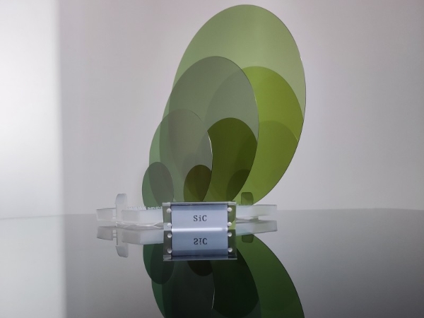
For high-quality semiconductor wafers with low surface roughness, JXT offers a range of high-precision sapphire wafers and silicon carbide wafers, available in sizes from 2 to 12 inches. JXT’s wafers, including both conductive and semi-insulating types, are manufactured to meet stringent surface requirements, making them ideal for applications in optoelectronics, semiconductors, and optics. The following is our silicon carbide double-polished wafer, with a roughness of less than 0.5 nm.

Related product links
Silicon Carbide Wafer (SiC Wafer)
As semiconductor technology advances, Gallium Nitride (GaN) has become a core material in optoelectronics, rad...
With the rapid advancement of third-generation semiconductor technologies, Silicon Carbide (SiC) has emerged a...
As third-generation semiconductor materials such as silicon carbide (SiC) and gallium nitride (GaN) continue t...
