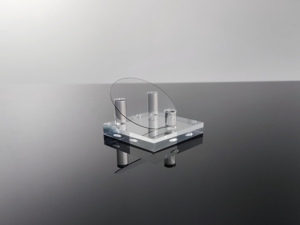
Gallium nitride (GaN) is a key wide-bandgap semiconductor material widely used in optoelectronics and high-power electronic devices. To meet the stringent requirements of these high-performance applications, the fabrication of high-quality GaN single-crystal substrates is essential. This article outlines the detailed fabrication process, including crystal acquisition, slicing, polishing, and surface treatment, with a focus on precision and quality control.
1. Acquisition of GaN Crystal
The fabrication of GaN single-crystal substrates begins with the growth of high-quality GaN crystals. Common growth techniques include HVPE (hydride vapor phase epitaxy), ammonothermal method, and Na-flux method. These methods produce bulk GaN crystals, which serve as the foundation for substrate processing.
HVPE: GaN is grown through a chemical reaction between gallium chloride (GaCl) and ammonia (NH₃) at high temperatures. This method is characterized by its high growth rate and relatively low defect density.
Ammonothermal Method: GaN is grown in a high-temperature, high-pressure ammonia environment using a solvothermal reaction, ideal for producing low-defect-density crystals.
Na-Flux Method: This involves the reaction of gallium with ammonia in a flux solution to deposit GaN crystals. It is cost-effective but limited in crystal size.
2. Crystal Orientation
Crystal orientation is critical to ensure the quality of subsequent substrate processing. X-ray diffraction (XRD) or Laue diffraction is employed to determine the orientation of the GaN crystal. The desired orientation (e.g., -plane, -plane, -plane) is selected based on application requirements. The -plane orientation is the most commonly used for optoelectronic devices and epitaxial growth.
3. Crystal Slicing
Slicing is a key step in transforming bulk GaN crystals into thin wafers.
Tools: High-precision diamond wire saws or inner diameter (ID) saws are used to ensure accuracy and flatness.
Process:
The bulk GaN crystal is securely mounted on a fixture to maintain stability and precise alignment.
The crystal is sliced into thin wafers with thicknesses typically ranging from 300 to 1000 µm.
Cutting speed and pressure are carefully controlled to minimize cracks or warping.
After slicing, the wafer surfaces are relatively rough and require further processing.
4. Planarization
Sliced wafers exhibit surface roughness and residual stress that must be addressed through grinding and planarization.
Coarse Grinding: Coarse diamond abrasives or slurry are used to remove surface damage and mechanical stress layers.
Fine Grinding: Finer abrasives are then employed to improve flatness and prepare the wafers for polishing.
Following grinding, the surface roughness is significantly reduced, but further polishing is required to meet the stringent requirements of semiconductor fabrication.
5. Chemical Mechanical Polishing (CMP)
CMP is a crucial step to achieve ultra-smooth surfaces with minimal defects.
Principle: A combination of chemical etching and mechanical abrasion removes surface irregularities and micro-defects.
Process:
A polishing slurry containing alumina or silica is applied, with controlled pressure and rotational speed.
Process parameters, including polishing time, pressure, and temperature, are carefully optimized to avoid introducing new damage.
After CMP, the surface roughness (Ra) of the GaN single-crystal substrate can reach 0.1-0.5 nm, meeting the requirements for high-quality epitaxial growth.

6. Surface Treatment
To further enhance surface quality and crystal performance, additional treatments are applied:
Chemical Etching: Hot phosphoric acid or hydrofluoric acid solutions are used to remove residual defect layers.
Ultrasonic Cleaning: Deionized water and ultrasonic cleaning remove particles and chemical residues from the substrate surface.
7. Substrate Dimensional Adjustment
Processed GaN wafers are adjusted to meet specific application requirements:
Diameter: Wafers are cut into standard sizes such as 2-inch, 4-inch, or 6-inch diameters.
Thickness: Thickness is adjusted to match the requirements for epitaxial growth or device fabrication, typically 100-500 µm.
Patterned Substrates (PSS): Micro- or nano-structures are created on the wafer surface using laser etching to improve the quality of subsequent epitaxial growth.
8. Quality Inspection
To ensure the substrates meet the stringent demands of semiconductor applications, rigorous quality inspections are conducted:
Surface Quality: Optical microscopy and atomic force microscopy (AFM) are used to check for surface defects, roughness, and scratches.
Crystal Quality: XRD is employed to measure crystal orientation deviation, while photoluminescence (PL) testing is used to assess defect density.
Warp and Stress: Interferometry or other optical methods measure wafer warp and residual stress.
9. Final Packaging
High-quality GaN single-crystal substrates that pass inspection are packaged in a cleanroom environment to prevent contamination or mechanical damage during transportation. The packaged substrates are ready for delivery to semiconductor manufacturers for use in advanced optoelectronic and power electronic devices.
Conclusion
The fabrication of GaN single-crystal substrates involves a multi-step, high-precision process. From the initial growth of GaN crystals to slicing, polishing, and surface treatment, each step plays a critical role in ensuring the final substrate's quality. Continuous optimization of fabrication techniques and defect density control is key to improving substrate performance, paving the way for their extensive use in next-generation semiconductor devices.
Related product links
As semiconductor technology advances, Gallium Nitride (GaN) has become a core material in optoelectronics, rad...
With the rapid advancement of third-generation semiconductor technologies, Silicon Carbide (SiC) has emerged a...
As third-generation semiconductor materials such as silicon carbide (SiC) and gallium nitride (GaN) continue t...
