Gallium arsenide (GaAs) is a compound semiconductor material known for its exceptional electronic and optical properties. As a III-V semiconductor, GaAs offers superior electron mobility, excellent high-frequency performance, and resilience in high-temperature environments. These advantages make GaAs substrates essential for the fabrication of advanced semiconductor devices, including microwave, millimeter-wave, optoelectronic components, and high-frequency power amplifiers. With the ongoing advancement of semiconductor technology, the industry has shifted towards larger wafer sizes, and 8-inch (approximately 200 mm) GaAs substrates are increasingly becoming the standard. This shift is driving the mass production and performance enhancement of GaAs-based devices.
 Substrate")
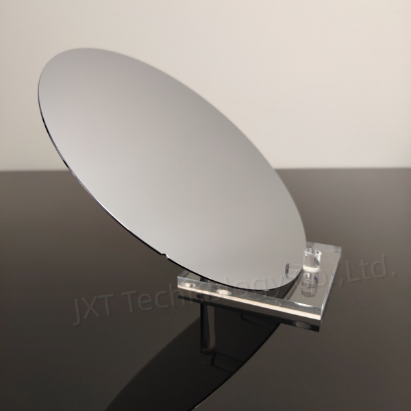
Advantages of 8-Inch GaAs Substrates
Larger Wafer Size for Higher Yield The transition to 8-inch GaAs substrates from smaller sizes such as 2-inch, 4-inch, and 6-inch wafers offers significant benefits in production efficiency. Larger wafers allow for the manufacture of more chips per substrate, reducing the cost per unit and improving overall throughput. This is particularly critical for high-frequency applications and large-scale integrated circuits where cost and efficiency are major concerns.
Superior Material Properties
High Electron Mobility: GaAs boasts electron mobility significantly higher than that of silicon, enabling faster switching speeds and lower power consumption, which are crucial for high-frequency and high-power applications.
Excellent High-Frequency Characteristics: GaAs performs exceptionally well in the microwave and millimeter-wave frequency ranges, making it ideal for devices used in radar systems, satellite communications, and emerging 5G technology.
Radiation Resistance: GaAs is highly resistant to radiation, making it suitable for use in aerospace and military electronics, where reliability in harsh environments is essential.
Optoelectronic Applications GaAs’s direct bandgap makes it an excellent material for optoelectronic devices such as light-emitting diodes (LEDs), laser diodes (LDs), and photodetectors. As the production of 8-inch GaAs substrates scales up, manufacturers can increase yield and improve the reliability of these optoelectronic components, further driving innovation in the fields of telecommunications, data transmission, and advanced imaging technologies.
Manufacturing Challenges and Solutions
The fabrication of 8-inch GaAs substrates presents significant technical challenges due to the brittle nature and mechanical limitations of GaAs compared to silicon. Key processes in manufacturing include crystal growth, cutting, grinding, polishing, and defect management. As wafer sizes increase, ensuring the structural integrity and quality of GaAs crystals becomes more demanding.
Crystal Growth: High-quality, large-diameter GaAs single crystals are grown using techniques such as Vertical Gradient Freeze (VGF) or Liquid Phase Epitaxy (LPE). These methods are critical for producing substrates with minimal defects and uniform electrical properties.
Processing Complexity: During cutting, grinding, and polishing, the brittle GaAs material is prone to cracking and other defects. This increases the complexity of manufacturing and can reduce yield. Therefore, optimizing these processes is essential to minimize material loss and enhance wafer quality.
The Future of 8-Inch GaAs Substrates
As demand for high-frequency, high-performance devices grows with the rise of 5G networks, IoT, and automotive radar systems, 8-inch GaAs substrates are becoming the industry standard. Advancements in manufacturing techniques are expected to lower production costs, making GaAs more accessible for a wider range of applications, including higher-frequency communication devices, precision sensors, and cutting-edge optoelectronics. This shift will enable greater device integration and miniaturization, driving innovation across various industries.
JXT Technology Co., Ltd: High-Quality GaAs Substrates
JXT Technology Co., Ltd is a leading supplier of high-quality GaAs substrates, including 8-inch wafers. The company employs advanced crystal growth and wafer processing technologies to ensure excellent uniformity, low defect density, and superior performance in high-frequency and optoelectronic applications. JXT Technology is committed to providing reliable and cost-effective solutions that meet the industry’s highest standards, supporting innovation and growth in the GaAs semiconductor market.
Conclusion
The 8-inch GaAs substrate is a key enabler of high-performance semiconductor devices, offering improved efficiency and scalability. With continued innovation, GaAs is set to play an essential role in future technology advancements. JXT Technology Co., Ltd remains at the forefront, delivering top-quality substrates that meet the evolving needs of the industry.
As semiconductor technology advances, Gallium Nitride (GaN) has become a core material in optoelectronics, rad...
With the rapid advancement of third-generation semiconductor technologies, Silicon Carbide (SiC) has emerged a...
As third-generation semiconductor materials such as silicon carbide (SiC) and gallium nitride (GaN) continue t...