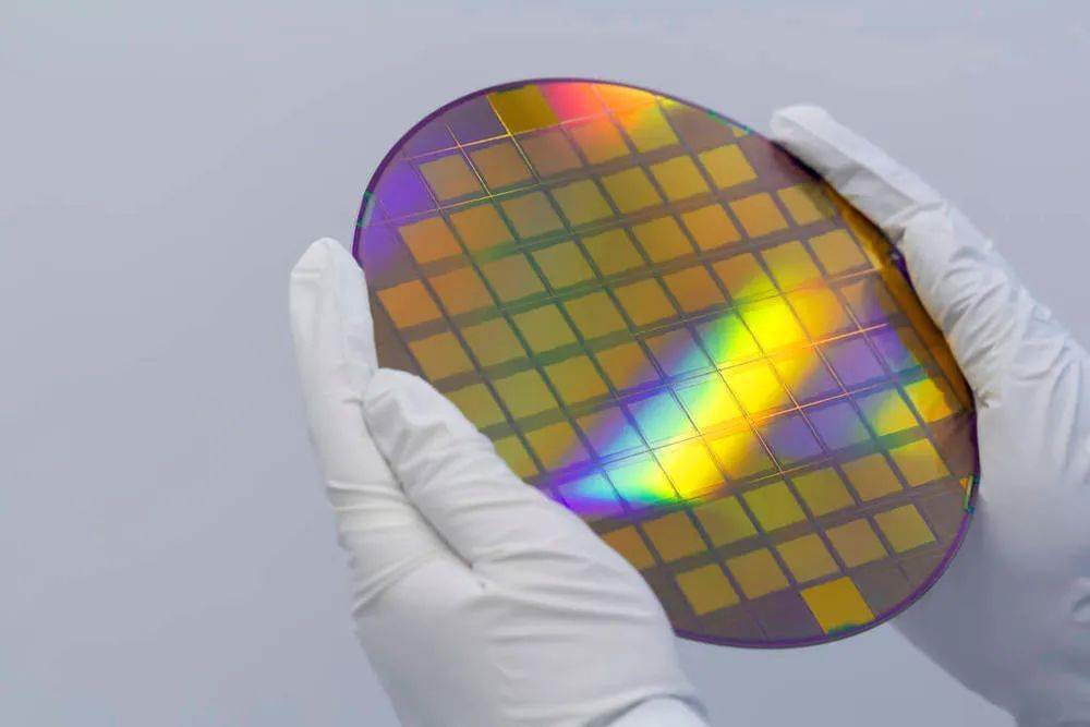
Gallium Nitride (GaN) Wafer is a wide-bandgap semiconductor material that exhibits unique optoelectronic properties, making it ideal for use in optoelectronic devices such as LEDs, lasers, and photodetectors. Some of the key properties of GaN wafer that make it an excellent material for optoelectronics include:
 Wafer")
Wide bandgap: GaN has a wide bandgap of 3.4 eV, which allows it to emit light in the blue to ultraviolet range.
High electron mobility: GaN has a high electron mobility, which means that it can transport electrons more quickly than traditional silicon-based materials.
High thermal conductivity: GaN has a high thermal conductivity, which allows it to dissipate heat more efficiently. This is important for optoelectronic devices that generate a lot of heat.
High saturation velocity: GaN has a high saturation velocity, which allows it to handle high current densities without suffering from electron "overflow."
These properties make GaN an ideal material for optoelectronic devices that require high power and high efficiency. For example, GaN-based LEDs are already being used in lighting applications because they offer higher energy efficiency, better color rendering, and longer lifetimes than traditional incandescent bulbs. In the future, we can expect to see even more applications of GaN-based optoelectronics, as researchers continue to explore this exciting material.
Gallium nitride (GaN) is a key wide-bandgap semiconductor material widely used in optoelectronics and high-pow...
GaN-on-Si LED epitaxial wafers are essential material platforms for high-performance optoelectronic devices. B...
In industries such as precision manufacturing, optics, semiconductors, and aerospace, surface roughness is a c...