Gallium Nitride (GaN) wafer technology is a relatively new field in semiconductor manufacturing, but it has quickly gained popularity due to its superior electrical and thermal properties. In this comprehensive guide, we’ll take a closer look at GaN wafer technology, its benefits, and applications.
 Wafer")
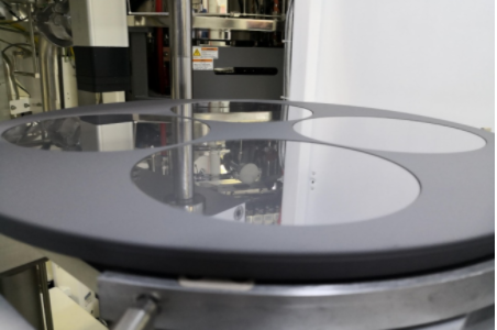
What are GaN wafers?
GaN wafers are made of Gallium Nitride (GaN), a wide-bandgap semiconductor material that has better electrical properties than Silicon (Si). GaN wafers are made by depositing GaN layers on a substrate (usually Silicon carbide (SiC) or Sapphire) using complex material growth techniques such as Metal Organic Chemical Vapor Deposition (MOCVD) or Molecular Beam Epitaxy (MBE).
Benefits of GaN wafers:
The benefits of GaN wafers include:
Higher electron mobility leading to better performance at higher frequencies
Higher breakdown voltage leading to better reliability and ruggedness
Lower on-state resistance leading to lower power loss
Higher thermal conductivity leading to lower operating temperatures
Higher efficiency leading to smaller system size and lower overall costs
Applications of GaN wafers:
GaN technology is widely used in many applications such as:
Power electronics: including power conversion (DC-DC converters, AC-DC converters), motor drivers and inverters
Solid-state lighting: including LED lighting and displays
RF and Microwave applications: including base station amplifiers and satellite systems
5G communications: including base station power amplifiers
Other applications such as medical electronics, electric vehicles, and aerospace and defense
Challenges in GaN Wafer technology:
Despite the many benefits of GaN wafers, there are some challenges that still need to be addressed, such as:
High material and manufacturing costs compared to traditional Si-based semiconductors
Non-standardized GaN wafer sizes, thicknesses, and specifications which can complicate manufacturing and design
Thermal management challenges due to the high thermal conductivity of the material
In conclusion, GaN wafer technology offers many advantages over traditional Si-based semiconductor materials, making it a promising option for various applications in power electronics, lighting, RF and microwave, 5G communications, and other industries. However, there are still challenges that need to be addressed to fully realize the potential of this technology.
Gallium nitride (GaN) is a key wide-bandgap semiconductor material widely used in optoelectronics and high-pow...
GaN-on-Si LED epitaxial wafers are essential material platforms for high-performance optoelectronic devices. B...
In industries such as precision manufacturing, optics, semiconductors, and aerospace, surface roughness is a c...